SPRADB7 September 2023 AM2431 , AM2432 , AM2434 , AM2631 , AM2631-Q1 , AM2632 , AM2632-Q1 , AM2634 , AM2634-Q1 , AM263P4-Q1 , AM2732 , AM2732-Q1
- 1
- Abstract
- Trademarks
- 1Introduction
- 2Thermal Resistance Overview
- 3Board Design Choices that Affect Thermal Performance
- 4Thermal Design Best Practices Review
- 5AM263x EVM Thermal Comparison with Data
- 6Using the Thermal Model
- 7References
3.1 Thermal Vias
The thermal via array implementation is arguably the most important aspect of thermal design for the AM263x since unless there is a heatsink used for the BGA package, the thermal vias are the only heat-sinking thermal connection for the BGA package. The thermal vias for the AM263x are in the form of the ground return vias attached to each VSS pin of the BGA.
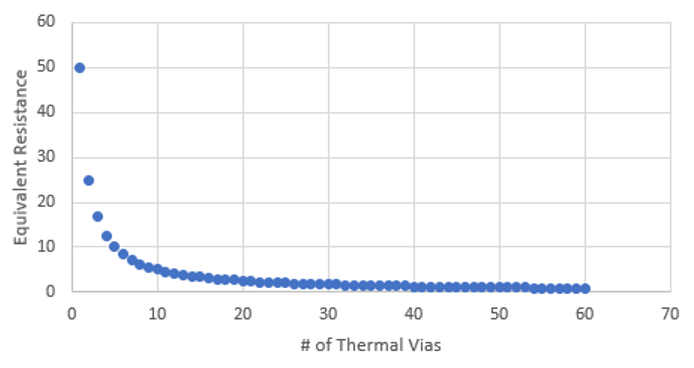
The thermal resistance of thermal vias (RΘvias) relates to the total thermal resistance of all thermal vias beneath the SoC. Each individual thermal via is analogous to a resistor where the equivalent resistance of all resistors is similar to many parallel resistors. Similar to an increasing number of parallel resistors and equivalent resistance, there are diminishing returns on the equivalent thermal resistance with each additional thermal via. For example, in a case where a single via has a thermal resistance of 50℃/Watt then Figure 3-1 shows the relationship between number of thermal vias and the equivalent thermal resistance (assuming that all vias have the exact same properties).
 Figure 3-1 Equivalent Resistance Graph for
Thermal Vias
Figure 3-1 Equivalent Resistance Graph for
Thermal ViasThe dimensions of a thermal via are what determine a single thermal via's thermal resistance. a general rule of thumb is that RΘvias is estimated by the following equation:
Where λ(Cu) is the conductivity of copper or 4 Watts per meter-kelvin, length refers to the length of the via, and the equation for thermal via area is:
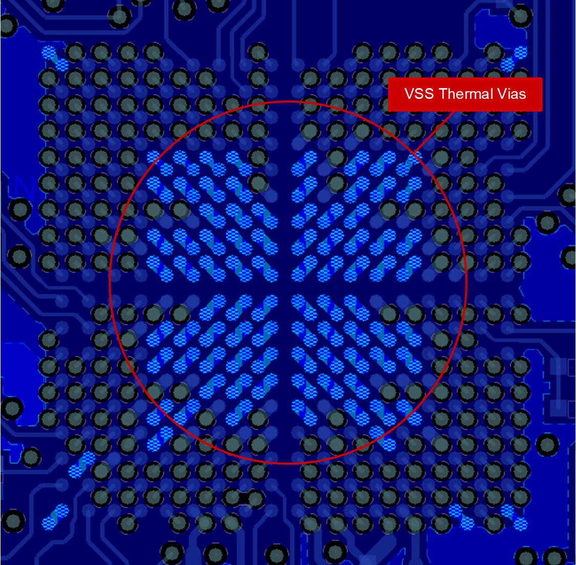
Figure 3-2 shows an example of the thermal via array with 8mil holes and 10 mil trace width from the BGA to the thermal vias.
 Figure 3-2 AM263x controlCARD Thermal
Vias
Figure 3-2 AM263x controlCARD Thermal
ViasFor best thermal performance:
- Use vias on each VSS pin of the BGA
- Use widest possible traces from the BGA to the via
- Use the largest possible drill diameter
- Conductively fill the thermal vias
| Measurement | TMDSCNCD263 | LP-AM263 |
|---|---|---|
| Number of thermal vias | 90 | 90 |
| Drill hole diameter | 8 mil | 8 mil |
| Plating Thickness | 35 um | 20-30 um |
| Conductively filled vias | Resin filled | Empty cavity |