SPRADF4 December 2023 TMS320F280023C , TMS320F280025C , TMS320F280025C-Q1 , TMS320F280037C , TMS320F280037C-Q1 , TMS320F280039C , TMS320F280039C-Q1 , TMS320F280049C , TMS320F280049C-Q1 , TMS320F28377D , TMS320F28377D-EP , TMS320F28377D-Q1 , TMS320F28377S , TMS320F28377S-Q1 , TMS320F28379D , TMS320F28379D-Q1 , TMS320F28379S , TMS320F28P650DK
3 Turn-On Delay Configurations
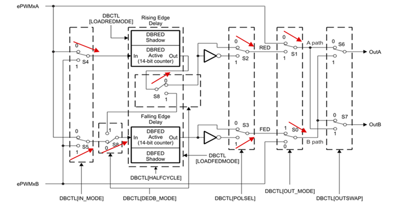
For most applications, users add the turn-on delay for the SR PWM with respect to the primary side PWM, and the DB submodule can be used. However, only the rising edge delay can be directly enabled for the AQ signal (EPWM2A) with the DB submodule. Thus, to further leverage the falling edge delay block for EPWM2B AQ signal, create the reversed polarity signal for the original AQ output, and reverse the signal back after adding the falling edge delay with the DB submodule. The detailed configurations are shown in Figure 3-1 with the added red arrows. These configurations allow users to add a turn-on delay with the existing rising and falling edge delay of the DB submodule for SR PWMs, EPWM2A, and EPWM2B, respectively.
 Figure 3-1 Dead Band Submodule
Configurations