SSZT279 july 2020 TPS55288 , TPS65987D
USB technology has evolved – from a data interface capable of supplying limited power to a primary power source with an interactive data interface. Today, many devices charge or get their power from USB ports contained in laptops, cars, aircrafts or even wall sockets.
Because of its compact size and ability to both deliver power and transfer data, USB Power Delivery (PD) has become a ubiquitous power socket for many small devices such as cellphones, laptops and other handheld devices, as shown in Figure 1.
 Figure 1 Example laptop docking station
with USB PD
Figure 1 Example laptop docking station
with USB PDUSB PD specifications define how USB devices can negotiate for more current and/or higher or lower voltages over a USB cable, using the USB Type-C CC wire as the communications channel. USB PD specifications allow devices with greater power requirements to get the power they require to operate from the bus voltage (VBUS) while negotiating with external power sources.
To facilitate optimum charging, a USB PD charger must use one of these two mechanisms:
- A list of fixed voltages, each with its own maximum current.
- A list of programmable voltage ranges, each with a maximum current (programmable power supply), where the device will request a voltage (in 20-mV increments) that is within the specified range and within the maximum current allowance.
In this article, I’ll show you how to optimize USB PD charging capabilities by adding a buck-boost converter to your design.
Shrinking your overall design footprint while delivering maximum charging efficiency
Synchronous buck-boost converters can convert a battery voltage or adapter voltage into power-supply rails. TI’s TPS55288, for example, can adjust the output power range from around 10 W to 100 W based on the input voltage. Through the I2C interface, the output voltage of the TPS55288 is programmable from 0.8 V to 21.26 V with a 20-mV step. The default output voltage is 5 V when the device is enabled, and can be used in a docking station, car charger, wireless charger or PC applications.
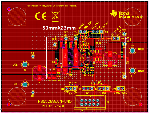 Figure 2 400-kHz EVM board solution size for the TPS55288
Figure 3 shows the conversion efficiency of the TPS55288 400-kHz EVM board in forced pulse-width modulation (FPWM) mode. When VIN ≥ 12 V, the conversion efficiency is higher than 95% at the 100-W output condition.
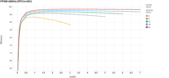 Figure 3 Efficiency vs. Output Current (FSW = 400 kHz, vOUT = 20 V)
Figure 4 shows the solution size of the TPS55288 2-MHz EVM board. When working in boost mode, the TPS55288 can deliver 60 W from a 12-V input with a 2-MHz operating frequency.
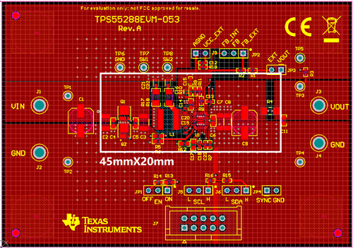 Figure 4 2-MHz EVM Board Solution Size for the TPS55288
Figure 5 shows the conversion efficiency of the TPS55288 2-MHz EVM board in FPWM mode. When VIN ≥ 12 V, the conversion efficiency is higher than 90% at the 60-W output condition.
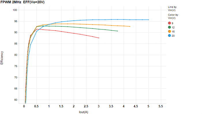 Figure 5 Efficiency vs. Output Current (FSW = 2 Mhz, vOUT = 20 V)
Improving thermal performance
Good thermal performance means higher reliability and longer lifetime for a product. Figure 6 is a thermal image of the TPS55288 400-kHz EVM board at 20-V/3-A and 20-V/5-A load conditions, respectively. The TPS55288 has only a moderate 40°C temperature rise at a 20-V/3-A load. Even at 100 W output power without a heat sink or thermal pad, the maximum temperature on the TPS55288 is only 86.4°C, much lower than the 150°C limit.
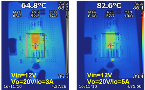 Figure 6 Thermal Performance (FSW = 400 Khz)
Achieving low EMI
A key design challenge for the power supply design is passing the electromagnetic interference (EMI) test. Circuits that fail the EMI test repeatedly often require round-the-clock efforts in the lab to fix the problem and avoid product launch delays. The TPS55288 buck-boost converter can achieve very good EMI performance. With frequency dithering function and by optimizing the placement and routing, the device can pass CISPR25 level 5 conducted emission and radiated emission limits, which are very strict.
 Figure 7 Conducted and Radiated EMI Results under FSW = 400 kHz (12 vIN, 15 VOUT/3 A)
 Figure 8 Conducted and Radiated EMI Results under FSW = 2 Mhz (12 vIN, 15 VOUT/3 A)
Benefits of a programmable output current-limit function
Besides high efficiency, small solution size and low EMI, other features make the TPS55288 a good fit for USB PD applications.
How are you designing with the TPS55288? Please add a comment below on how you’re using the device, and how it’s shortening your design time.
Additional resources
Read these application reports: