SSZT291 june 2020 CSD17381F4 , CSD17382F4 , CSD17578Q5A , CSD23382F4 , CSD25310Q2 , CSD25480F3 , CSD25481F4
Power metal-oxide semiconductor field-effect transistors (MOSFETs) use a thin oxide to isolate the gate electrode from the active area of the transistor. Much like the MOSFET structures used in the fabrication of microprocessors, a power MOSFET gate oxide is just as susceptible to damage from electrostatic discharge (ESD) as its tinier counterparts. ESD may cause catastrophic failure (such as gate-oxide breakdown) or non-catastrophic damage.
Some discrete power MOSFETs and power-block MOSFETs include integrated ESD protection structures to prevent unwanted MOSFET failures caused by ESD. In this article, I’ll explain the differences between the ESD structures used in power MOSFETs and look at design considerations for these devices.
ESD structures used in TI MOSFETs
First, let’s look at the three protection categories into which discrete power MOSFETs and power-block MOSFETs fall: no ESD protection, single-ended ESD protection and back-to-back ESD protection.
No ESD protection
The first category is self-explanatory and makes up the bulk of power MOSFET and power-block MOSFET products offered by TI and other vendors. Although these MOSFETs do not have an integrated gate ESD structure, they still have an inherent ESD capability that can range from as low as 150 V to as high as 3,000 V. The ESD capability is related to device density and charge; as such, larger die sizes have higher ESD capabilities.
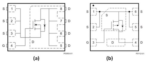
You should always confirm that the MOSFET’s ESD capability meets the requirements in your application; if it does not, consider adding external ESD protection. Figure 1 illustrates the schematic symbols for TI N-channel and P-channel MOSFETs with no integrated ESD protection.
 Figure 1 MOSFETs with no ESD protection: N-channel (a); and P-channel (b)
Single-ended ESD protection
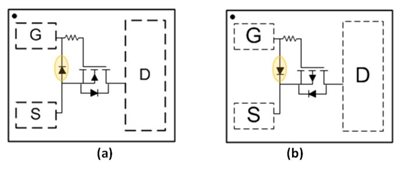
The second category includes N-channel and P-channel MOSFETs with an integrated, single-ended ESD protection diode from gate to source. Devices in this category can achieve ESD ratings >4,000 V. Historically, ESD protection of a power MOSFET gate resulted in higher gate leakage current. However, some devices, including TI’s CSD25480F3, can now achieve industry-leading leakage specifications as low as 25 nA; these are better specifications than devices with no gate ESD!
Because of their low gate leakage, TI MOSFETs are a good fit for battery-powered applications where standby power and runtime are critical. You must carefully evaluate operating conditions to ensure that the ESD diode is not forward-biased, as it will conduct current. If forward-biasing is unavoidable, then I recommend including an external, current-limiting gate resistor in the circuit. Figure 2 shows N-channel and P-channel schematic symbols with the single-ended ESD protection diode highlighted.
 Figure 2 MOSFETs with single-ended ESD protection: N-channel (a); and P-channel (b)
Back-to-back ESD protection
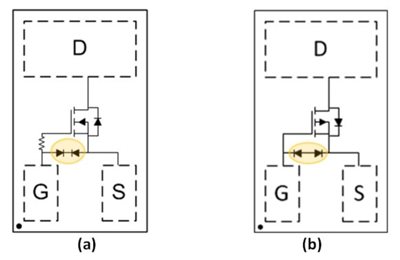
The final category includes N-channel and P-channel MOSFETs with a back-to-back ESD protection structure. The ESD capability of these devices ranges from 400 V up to 3,250 V. There is no need to worry about forward-biasing the back-to-back ESD structure, but these MOSFETs have higher gate leakage current than MOSFETs with single-ended ESD protection. This higher gate leakage may be a drawback in battery-powered applications. Figure 3 shows N-channel and P-channel schematic symbols with back-to-back ESD protection highlighted.
 Figure 3 MOSFETs with back-to-back ESD protection: N-channel (a); and P-channel (b)
Examples of ESD ratings and leakage current for TI MOSFETs
Table 1 lists some examples of the human body model (HBM) and charged device model (CDM) ESD ratings and maximum gate leakage current for N-channel and P-channel TI MOSFETs in each category.
| Part number | N-channel or P-channel | ESD protection category | HBM ESD rating (V) | CDM ESD rating (V) | Maximum IGSS (nA) |
|---|---|---|---|---|---|
| CSD17578Q5A | N | None | 600 | 2,000 | 100 |
| CSD25310Q2 | P | None | 250 | 1,500 | -100 |
| CSD17381F4 | N | Single-ended | 7,000 | 2,000 | 50 |
| CSD25481F4 | P | Single-ended | 4,000 | 1,000 | -50 |
| CSD17382F4 | N | Back-to-back | 3,000 | 2,000 | 5,000 |
| CSD23382F4 | P | Back-to-back | 2,000 | 2,000 | 10,000 |
Conclusion
Discrete power MOSFETs and power-block MOSFETs offer different categories of gate ESD protection. Each category has trade-offs in terms of ESD protection levels and gate leakage current. Knowing these trade-offs can help you make informed decisions when selecting a MOSFET for your application.
As a helpful reminder, look for the schematic illustration, which depicts the type of ESD protection included in a particular device, on page 1 of TI MOSFET and power-block data sheets.
Additional resources
- Visit the TI MOSFET support and training center.
- Read the application report, “Electrostatic Discharge (ESD).”