SSZT343 February 2020 LM34936 , LM5175 , LM5176
For applications using USB Type-C Power Delivery (PD) and wireless charging, the output voltage (VOUT) from the charger can fluctuate higher or lower than the input voltage. Four-switch buck-boost regulators are popular in these applications because adjusting their feedback signal can dynamically change the VOUT.
A buck-boost regulator’s output voltage can be adjusted either by varying the error amplifier’s reference voltage (VREF) or by varying the feedback voltage. If monolithic pulse-width modulation (PWM) four-switch buck-boost controllers such as TI’s LM34936 and LM5176 do not provide the ability to access VREF, however, varying the feedback voltage becomes the only way.
To help you design systems using buck-boost controllers with dynamic output voltages, in this series I will discuss a few options for using the feedback signal to adjust the output voltage. The first installment will focus on using switched resistors, while the second installment presents a different approach that requires fewer components and signal lines.
Understanding the VOUT setting and feedback signal
Figure 1 shows a typical VOUT setting for the controller and error amplifier. By looking up the VREF for the error amplifier in the data sheet, Equation 1 calculates VOUT by setting the values of R1 and R2:
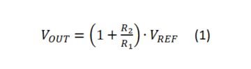
 Figure 1 Feedback Circuit and
vOUT Setting
Figure 1 Feedback Circuit and
vOUT SettingUsing switched resistors to adjust VOUT
Figure 2 shows a simple option to dynamically adjust VOUT between two voltage levels by incorporating a switch, S1. Assume that S1 is an ideal switch, and that its impedance is infinity when off and 0 Ω when on. When switch S1 is turned off, R3 is not in the picture of the VOUT setting, and is simply the same as given in Equation 1. To avoid confusion in this discussion, let’s assume that the voltage is VOUT1, as expressed by Equation 2:

If S1 is turned on, it will place R3 in parallel with R1. The new output voltage, VOUT2, will satisfy Equation 3:

where
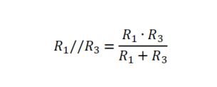
This results in VOUT2 being greater than VOUT1. By solving Equation 2 and Equation 3, you can determine the resistor values. By toggling S1, you can switch VOUT between VOUT1 and VOUT2.
 Figure 2 VOUT Adjustment
with a Switched Resistor
Figure 2 VOUT Adjustment
with a Switched ResistorPreventing a false OVP trigger
Some PWM controllers like the LM34936 and LM5176 have built-in output overvoltage protection (OVP), implemented by monitoring the feedback (FB) pin voltage. If the FB pin sees >10% above VREF, the controller riggers OVP and stops switching until after the FB voltage falls below the hysteresis of the OVP threshold. Because of this feature, any abrupt resistor switching should be prevented, since turning off S1 suddenly will cause the FB voltage to jump up instantaneously and create a false OVP event. The solution is to switch S1 gradually, where R5 and C1 delay the on/off command of S1 to engage or disengage R3 gradually.
There are a couple of factors involved in selecting the resistor-capacitor (RC) delay time constant; the RC needs to match up with the loop response time, as well as the transition time between VOUT levels specified by the application, in order to enable proper transition between the two voltage outputs.
Multivoltage programming
Adding switched resistor branches can program additional VOUT levels. Figure 3 shows an approach employing three switched resistor branches to set the four VOUT levels for USB Type-C PD applications.
 Figure 3 Three Switched Resistor
Branches for Four vOUT Settings
Figure 3 Three Switched Resistor
Branches for Four vOUT SettingsTable 1 summarizes the programming schemes for the four different voltages.
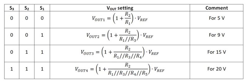
Table 1: Programming switched resistors for USB Type-C PD
As shown in Figure 4, it is important to make sure that switching to different resistors won’t trigger a false OVP event in the feedback loop. Incorporating an RC for each of the switches will help avoid an OVP event while switching to the proper voltage rail at the appropriate time.
 Figure 4 Gradually Switching the
Resistor to Avoid Triggering an OVP Event During Dynamic vOUT
Adjustment
Figure 4 Gradually Switching the
Resistor to Avoid Triggering an OVP Event During Dynamic vOUT
AdjustmentConclusion
By incorporating switches and resistors into the feedback loop, buck-boost converters can dynamically adjust the VOUT for USD Type-C PD and wireless charging applications. This approach is straightforward, simple and easy to implement. Controlling the speed of the switches is a requirement when using four-switch buck-boost controllers.
For a different approach using fewer components and signal lines, see the second installment of this series.
Additional resources
- See TI’s USB Type-C PD reference designs at www.ti.com/product/LM5175/toolssoftware
- Check out the LM34936 and LM5176 controller data sheets.