SSZT428 August 2019 INA818 , INA819 , INA821 , INA828 , INA848 , INA849
An instrumentation amplifier (INA) is a very special type of differential input amplifier; its primary focus is to provide differential gain and high common-mode rejection. INAs offer high input impedance and low output impedance; newer devices will also offer low offset and low noise.
The unique combination of a high common-mode rejection ratio (CMRR) and high accuracy make INAs especially attractive for applications with small error budgets such as motor controllers, battery test equipment, analog input modules, LCD test equipment and patient monitoring systems. In order to understand why INAs fit well into these applications, it is important to discuss what an INA is and how it works.
First, let’s talk about what an INA is. The general definition of an INA is a circuit or device fitted with one to three internal operational amplifiers (op amps) to improve signal quality and increase common-mode rejection. The more common type of INA is the three op-amp configuration shown in Figure 1. This configuration can be set up discretely, but using an INA integrated circuit (IC) will not only save space in your design, but will reduce CMRR errors.
There are three main characteristics of this type of INA:
- The gain can be set by one external resistor, .
- The input stage is fitted with buffer amplifiers.
- The output stage is a traditional difference amplifier.
Understanding these three INA characteristics is the key to understanding how an INA works.
 Figure 1 INA Internal Stage
Diagram
Figure 1 INA Internal Stage
DiagramFirst, why is setting the gain using an external resistor so useful? The real question is, how is it not? Instead of elaborate feedback loops, you can save space in your design by just using one resistor and one INA.
So now you might question the input buffer stage. Why include the input buffers when you could just have the difference amplifier? There are two main reasons. Sensors and sensing circuity can have high output impedance. If the impedance is too high, it will dominate the input impedance of the difference amplifier. Designers isolate high impedance with a buffer. Since an op amp has high input impedance and low output impedance, TI placed the buffer stage before the difference amplifier to allow board- and system-level engineers to use any peripheral component with a TI INA. Another reason for the input buffer stage is that it sets the gain for the circuit.
The final stage of an INA is the difference amplifier. This is the part of the amplifier that rejects the common-mode voltage. This stage subtracts the two input signals. In a stand-alone difference amplifier, R2 and R4 would be equal, as would R1 and R3; and these resistors would set the gain. But in instrumentation amplifiers, the gain is set by the input stage, so R1 through R4 are equal for a gain of 1 V/V. Figure 1 expresses the gain of a difference amplifier as:
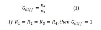
You only need the external resistor to determine the gain.
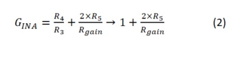
Equation 2 expresses the gain for a complete INA. The value of R5 will be listed in the INA’s data sheet.
So what on earth are INAs good for? INAs offer high CMRR, which is especially useful in noisy conditions and where there is common noise present across both input terminals. Here’s how that works out mathematically.
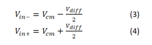
The input voltages are set to. The input feeding into U2 is and U3 is . The input voltages equate to Equations 3 and 4:
Equations 5 and 6 calculate the nodal voltages at the end of the input buffer and gain stage as:
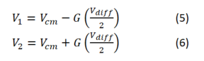
where . can be used for and , since R5 and R6 are set to equal values.
V1 and V2 are then fed into the difference amplifier stage, which results in Equations 7 and 8 (remember that the gain of the difference amplifier is usually 1):
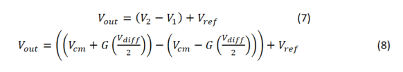
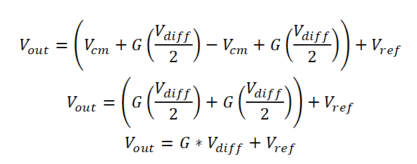
The first thing that you should notice is that the common-mode voltage cancels. It is common to set the reference voltage to ground, so all you are left with is the gained differential signal with respect to the reference voltage. The calculation below simplifies Equation 8 to show the final, ideal equation.
In a perfect world, the common-mode voltage would now be cancelled out, but that is not the case. CMRR error is dominated by resistor mismatch, primarily on the output difference amplifier, since that is where the common-mode rejection occurs. Resistor matching is more precise on an INA IC than on a discrete INA. You can reduce CMRR errors by increasing the gain on the input stage, but for lower gains, INA ICs are the better option. Even with errors, CMRR is still high for INAs.
Because of the high common-mode rejection, INAs are great to use when you need precise signals in the presence of common noise. For example:
- In industrial process control, industrial machinery often needs to do precise, repetitive tasks with little room for error. Noise in the industrial process can come from anywhere, such as the power line. INAs enable the precision and common-mode noise rejection needed to reduce errors in machinery.
- In medical applications, any error measurement in electrocardiograms and other patient monitoring systems could result in a false diagnosis. The measured signal is in the range of few millivolts with 50/60Hz common mode interference. INAs offer a gain error as low as 0.01% and an offset voltage in the microvolts range. This high level of accuracy is excellent for patient monitoring systems.
- In battery-powered instruments requiring single-ended signals and current sensors for the battery, INAs can convert a differential input signal to a single-ended output signal while drawing little quiescent current.
- In measurement systems, INAs are great for sensing current from various sensor applications.
- In motor controllers, getting a motor to do exactly what you want it to do requires accurate signals. INAs maintain low offset and gain error to condition signals for accurate position feedback.
As I mentioned, INAs work very well to convert differential signals into single-ended signals. Single-ended signals only require one wire in reference to another, meaning that multiple single-ended signals are all in reference to the same wire. This reduces the amount of wires in a design.
Single-ended signals are beneficial because many analog-to-digital converter (ADC) applications require a single-ended signal to operate. For this reason, INAs work well as an ADC driver for systems that take a sensor input. ADCs cannot accept a high common-mode voltage; INAs solve this problem by reducing the common-mode voltage so that the ADC can operate.
Table 1 lists some of TI’s newest precision INAs.
| Device | Description |
|---|---|
| INA818 | 35-µV offset, 8-nV/√Hz noise, low-power precision instrumentation amplifier |
| INA819 | 35-µV offset, 8-nV/√Hz noise, low-power precision instrumentation amplifier |
| INA821 | 35-µV offset, 7-nV/√Hz noise, low-power precision instrumentation amplifier |
| INA828 | 50-µV offset, 7-nV/√ Hz noise, low-power precision instrumentation amplifier |
| INA848 | 35-µV offset, 1.5-nV/√ noise, high-bandwidth, precision instrumentation amplifier |
| INA849 | 35-µV offset, 1-nV/√ noise, high-speed, precision instrumentation amplifier |