SSZT595 november 2018 TPS61372
Solid-state drive (SSD) storage is becoming more popular in PC, data-center and telecom applications, offering the benefits of faster speeds and a more compact size compared to Hard Disk Drive (HDDs). The new Peripheral Component Interconnect Express (PCIe) Non-Volatile Memory Express (NVMe) Host Controller Interface Specification SSD offers three times faster write speeds and six times faster read speeds compared to traditional Serial Advanced Technology Attachment (SATA) SSDs.
However, increasing Not-AND (NAND) flash write and erase speeds, as well as solving the thermal dissipation, impose big challenges on SSD designs.
A power supply is required to support the write/erase of the NAND chip, as shown in Figure 1.
 Figure 1 Write/erase the NAND Flash Cell
Equation 1 calculates the current during write/erase as:
I = C * (dVs / dt) + (Vs / R) (1)
For instance, if C is around 100 pF, R is around 1 MΩ. If write/erase completes in 100 ns, the current is around 12 mA. For an application like enterprise storage, a larger capacitance (increasing C) and faster speeds (decreasing t) require a higher current. The write/erase speed really depends on the power-supply capability and the overall thermal dissipation. If the power capability cannot deliver the required current due to current capability, the write/erase speed will scale down which in return impacts the response time of the storage system.
Charge-pump Converters vs. Inductive Boost Converters
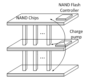
There are two basic types of step-up converters: a charge-pump converter and an inductive boost converter. Since charge-pump converters don’t use an inductor, the solution area for a charge-pump converter is relatively smaller and could be put into a NAND cell, as shown in in Figure 2.
 Figure 2 Traditional NAND Flash Chips
with an In-cell Charge-pump Converter
Figure 2 Traditional NAND Flash Chips
with an In-cell Charge-pump ConverterThe charge pump solution for applications with higher output-power requirements needs a larger capacitance due to charging/discharging capacitance with heavier load. The efficiency at heavy loads is also relatively low due to the power loss of the charging/discharging capacitor. Additionally, there are high output ripples and noise as well at heavier load conditions. Based on the limits of lower current capability, the charge-pump converter is a good fit for relatively lower-power applications, while being easy to design (since there is no inductor) and having a small solution size with medium-level efficiency.
In contrast, an inductive boost converter can deliver more current than a charge-pump converter and will have lower ripple, which makes it a more competitive solution for higher-power applications. The output voltage of the boost converter could be flatter across the whole load range as the inductor current could deliver the load current. As shown in Figure 3, placing a single boost converter outside of NAND chips could supply the power of multiple chips.
 Figure 3 NAND Flash Chips with an
Inductive Boost Converter
Figure 3 NAND Flash Chips with an
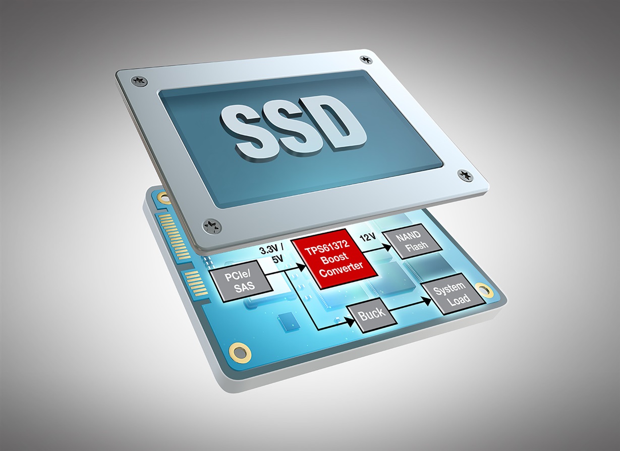
Inductive Boost ConverterThe TPS61372 synchronous boost converter could be a good fit for supplying the power to write/erase NAND chips in SSDs. It has a compact solution size and minimizes the need for external components. Compared to traditional charge-pump converters, the TPS61372 can deliver a higher-quality power supply to write/erase NAND chips.
Additional Resources
- Download the TPS61372 data sheet.
- Order the TPS61372 evaluation module.