SSZT714 May 2018 TPS62136 , TPS63710 , TPS82130
When looking for a DC/DC converter to create a negative voltage, in many cases you will use a step-down converter in the inverting buck-boost topology. While dedicated inverter devices such as the very-low-noise TPS63710 are easier to design with and generally a better solution, there are numerous reasons to use a step-down converter as an inverting buck-boost converter instead. First, there are relatively few dedicated voltage inverter devices in the market, compared to the ubiquitous step-down converter. You may not find a specific feature or characteristic which is required in your application. In other cases, it greatly simplifies the procurement effort to use another instance of an existing step-down converter for another socket in the design through utilizing it in the inverting buck-boost topology. Since there are generally very few inverting buck-boost circuits available for lab testing, you will need to modify the readily-available step-down converter EVM into the inverting buck-boost topology to measure the circuit for your design. This blog walks you through the steps required to take the standard TPS82130 evaluation module (EVM), which is configured as a step-down converter, and create an inverting power supply based on 3- to 11.5-VIN, –5-VOUT, 1.5-A Inverting Power Module reference design.
Using a step-down converter as an inverting buck-boost converter is a valid application use case, supported by numerous reference designs and applications notes. The TPS82130 step-down power module is used as the example, because of its high integration level and simple design. It also contains two inverting buck-boost reference designs, TIDA-01457 and TIDA-01405, with full test data and documentation. Please see the reference design guide section 2.3 for a detailed technical discussion of using step-down converters as inverting buck-boost converters.
To begin, Figure 1 shows the standard EVM as it would be connected as a step-down converter.
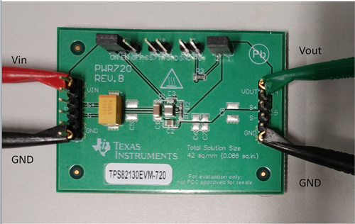 Figure 1 TPS82130EVM-720 Connected as a
Step-down Converter
Figure 1 TPS82130EVM-720 Connected as a
Step-down ConverterTo achieve the TIDA-01457 design, its inverting schematic in Figure 3 is compared to the normal step-down EVM’s schematic in Figure 2.
 Figure 2 Step-down Converter
(TPS82130EVM-720) Schematic
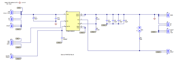 Figure 3 Inverting Buck-boost
(TIDA-01457) Schematic
Figure 3 Inverting Buck-boost
(TIDA-01457) SchematicTo achieve the inverting function, the output terminals are swapped such that VOUT (J4) becomes GND and the GND terminal (J6) becomes –VOUT. Everything that was GND is now labeled –VOUT. In addition, the input voltage is applied from VIN to VOUT, which is now GND.
Further comparing the two schematics, we find the remaining changes required to transform the EVM into the inverting circuit. Note that the reference designators are identical between the designs, except for the input capacitors C1 and C4 whose connections need to change from what the existing printed circuit board (PCB) provides.
Here are the required changes, which are shown in the following images:
- Remove C1 and C4, but save them to re-install later
- Install a 22-µF ceramic output capacitor at C6, C7, and C8
- Change the value of R1 and R2 to set the appropriate output voltage
- Install the input capacitors, C10 and C11, which were saved from earlier
First, the input capacitors are removed, the additional output capacitors installed, and the two feedback (FB) resistors changed. Figure 4 shows the resulting EVM:
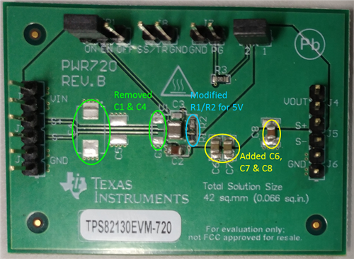 Figure 4 TPS82130EVM-720 Partially
Modified to an Inverting Circuit
Figure 4 TPS82130EVM-720 Partially
Modified to an Inverting CircuitNext, the input capacitors, C10 and C11, are installed. There are no pads at the correct electrical locations on the existing EVM, so the existing pads for the VIN connection are used and a wire is added to complete the connection to GND, which is VOUT on the PCB. Figure 5 shows the result, which has completed all modifications and is now an inverting buck-boost power supply.
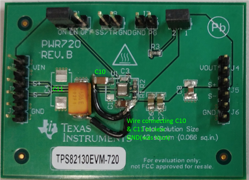 Figure 5 TPS82130EVM-720 Completely
Modified to an Inverting Circuit
Figure 5 TPS82130EVM-720 Completely
Modified to an Inverting CircuitFigure 6 shows this same EVM wired in the correct way and ready to be powered on. Note that the positive terminal of the load connects to GND (J4) and the negative terminal to GND (J6). This presents the load with a positive voltage, instead of a negative one.
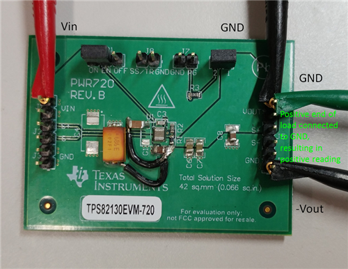 Figure 6 TIDA-01457 Connected as an
Inverting Buck-boost Converter
Figure 6 TIDA-01457 Connected as an
Inverting Buck-boost ConverterThese same steps and procedures are applicable to most step-down converter EVMs and allow you to quickly evaluate them as inverting buck-boost converters, without having to make a PCB of your own.
Additional Resources
- Browse TI’s inverting charge pump solutions.
- Browse TI’s inverting buck-boost solutions.