SSZT804 february 2018 TPS22918
If you're designing systems with complex processors, the chances are high that you'll have to consider power sequencing. Power sequencing is necessary in many systems during power up and/or power down phases, however,the timing requirements vary depending on processor selection and the subsystems being powered. For example, the image processor in a multifunction printer (MFP) has several rails that need to power up and power down in a specific order. This order ensure that the internal circuitry is properly biased and staggers the in-rush current at startup. In this post, I will review different ways to implement power sequencing and the benefits of using integrated load switches to do so.
Why Use Load Switches for Power Sequencing?
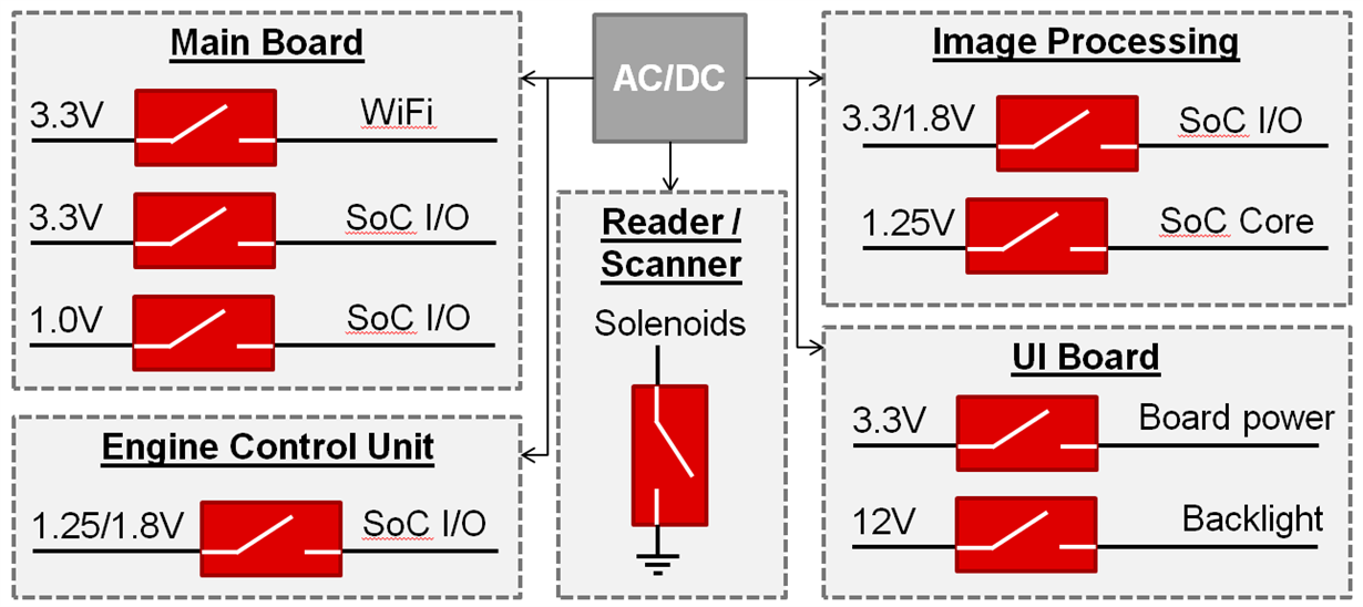
Load switches are a great potion for power sequencing in your designs because they provide flexibility and increased protection in a smaller solution size. Design flexibility and simple control of subsystem power sequencing. Each rail can turn on and off independently without extensive processor intervention, and the rise and fall time of each rail is adjustable. This is possible because of features available in integrated load switches such as configurable rise time and quick output discharge (QOD). The TPS22918 is an example of an integrated load switch that has both of these features available. Figure 1 shows examples of common subsystems.
 Figure 1 General System Block Diagram
of MFP Subsystems
Figure 1 General System Block Diagram
of MFP SubsystemsAdditionally, using load switches instead of discrete metal-oxide semiconductor field-effect transistor (MOSFET) solutions also provides improved transient behavior and smaller solution size; you can read more about these benefits in the application report, “Integrated Load Switches Versus Discrete MOSFETs.”
And if you need more protection throughout your design, load switches can help here too. You can place an eFuse at the input of any hot-pluggable loads to help against hot-plug transients and protect downstream DC/DC converters from an input voltage that is too high or too low. Unlike a discrete fuse, eFuses do not need replacing after a fault, resulting in reduced system downtime and decreased maintenance costs.
Power Sequencing Configuration Options
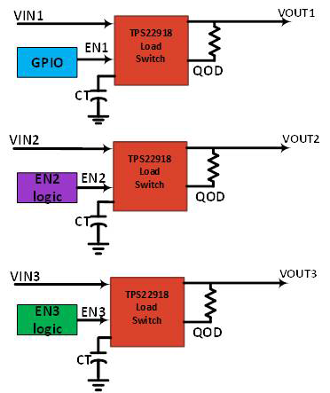
We understand that power sequencing requirements are unique to each processor and system configuration; load switches are adaptable to numerous configuration options as seen below. Load switches control each power rail by adjusting the timing capacitance value on the CT pin and the resistance value on the QOD pin, without the need for external digital components such as oscillators, clocks or a processor. Figure 2 shows various configurations for implementing power sequencing in your system.
 Figure 2 General-purpose Input/output
(GPIO) Configuration
Figure 2 General-purpose Input/output
(GPIO) ConfigurationFigure 2 uses independent enables for each load switch to trigger power-up sequencing while varying the resistance on the QOD pin achieves power-down sequencing.
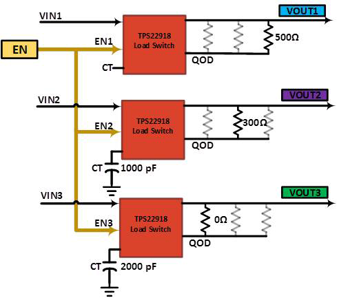
Figure 3 uses one GPIO signal to enable all three load switches, but varies the capacitance at the CT pin to control power-up sequencing. Again, varying the resistance on the QOD pin achieves power-down sequencing.
 Figure 3 CT Configuration Block
Diagram
Figure 3 CT Configuration Block
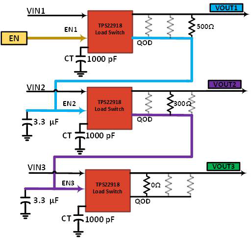
DiagramFigure 4 routes the QOD output of the previous load switch to the enable pin of the next load switch. Adding an external resistor-capacitor (RC) in parallel to the QOD output achieves power-up sequencing. Once more, varying the resistance on the QOD pin achieves power-down sequencing.
 Figure 4 QOD Configuration
Conclusion
As we've discussed in this blog, power sequencing enables you to create a configuration that fits your needs while remaining simple, small and protected. You can learn more about implementing power sequencing in your designs from TI’s Power Sequencing Reference Design Using Load Switches. Since timing constraints vary greatly between different applications and processor-to-processor communications, this reference design is not limited to one specific timing sequence. Instead, the design enables you to configure multiple timing configurations to fit system specifications.
Additional Resources
- Only have a few minutes? Watch some videos:
- “Load Switches vs. Discrete MOSFETs” (2:35).
- “Load Switches vs. Discrete MOSFETs – Problems with a discrete solution
and how a load switch can fix them” (3:22).
- Learn more about load switches by downloading these application notes:
- “Basics of Power Switches.”
- “Load Switches: What Are They, Why Do You Need Them and How Do You
Choose the Right One?”
- Check out the blog post, “What is a Load Switch?”