SSZT899 November 2017 LMZ31520
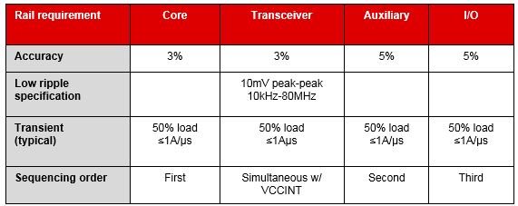
In the first installment of this series, I reviewed the system architecture choices for a field-programmable gate array (FPGA) power design and how to estimate the power requirements. Now that you have a good idea from the vendor’s spreadsheet what the voltage and current requirement of each individual rail is, you need to look at the requirements of each individual rail before selecting parts. In this installment, I will focus on the four basic types of rails: core, transceiver, auxiliary and input/output (I/O) rails. This is not an all-inclusive list of the rails that your specific FGPA may have, but they are the most common and each has distinct requirements. Table 1 summarizes the requirements for each rail.
|
Let’s start by looking at the core power rail. Typically, the core rail has a low voltage requirement but requires a high amount of current. Sequencing is also an important concern for this rail. Every FPGA must turn on and off in a certain order to satisfy each rail in the correct order. The core rail is typically the first rail on and the last rail off, so you should use a dedicated power supply for the core rail. I will go into more detail on sequencing techniques in the next blog. Finally, the core rail typically has a tight output-voltage tolerance requirement. It must have an accuracy of at least 3% (some FPGA families may be okay with 5% accuracy for the core rail) and be able to handle a 50% load step at <1A/µs.
The transceiver rail has the strictest requirements of all the rails on the FPGA. It typically has the tightest requirements for tolerance and requires an accuracy of 2.5-3%. This rail has strict noise requirements, requiring a voltage ripple of 10mV peak-peak or less over a wide range of frequencies. Thus, you may need a dedicated power supply for this rail, even if it has the same voltage requirements as another rail. Make sure to design the power supply for low noise, or simply choose a power module with guaranteed electromagnetic interference (EMI) performance. The layout of the power supply is also very important to help achieve low-noise targets. Make sure that your layout is tight, with capacitors close to the device pins.
The auxiliary and I/O rails typically have similar requirements, so I’ll discuss them together. Often, the same devices may power both rails. The current requirements of the I/O rail will vary depending on how many I/O banks you are using in your application, but typically the current requirements are lower than the core rail. The auxiliary and I/O rails have a looser tolerance requirement and can typically use devices with up to 5% accuracy.
Several times in this post, I’ve mentioned the importance of output voltage tolerance. It is important to consider the tolerance in two states: the static and dynamic state. As you can see in Figure 1, in the static state (when only fixed or gradual changes are occurring), the tolerance is made out of the voltage ripple and the power-supply regulation. Typically, it is at 1% or 1.5%. Next, you need to consider the tolerance in the dynamic state (when quick changes are occurring). The dynamic state is primarily made up of transient droop and DC loss.
Figure 1, using the LMZ31520 as an example, shows all of the factors that add up to create a static output voltage tolerance of 1.65%. This leaves about 1.35% of space to cover dynamic changes.
 Figure 1 Output Voltage
Tolerance
Figure 1 Output Voltage
ToleranceThere are many ways to improve the tolerance. In the static state, you can take measures to improve the power-supply regulation. Selecting a feedback resistor with a tight tolerance can help improve the overall tolerance. Additionally, you can reduce the output-voltage ripple by increasing the switching frequency you are using and adding additional ceramic output capacitors.
You can take steps to improve tolerance in the dynamic state. Transient droop occurs when the power supply changes state. The load-step size, load-step speed and output capacitance all affect the amount of transient droop. If the load step is small, the droop will be small. If the load step is large but the speed of the change is slow, the power supply can handle the change more easily and the droop will be small.
Even if the load step is large, you can still make quick improvements by adjusting the amount of output capacitance. Place bypass capacitors directly at the FPGA pins. Typically, the FPGA vendor will provide recommendations for the amount of capacitance needed. You can also use bulk capacitors to support load steps during power up or during changes in the processor state. Make sure to choose high-quality capacitors with low equivalent series resistance (ESR), like ceramic X5R or X7R dielectric capacitors. Adding different types of capacitors can also help. Bulk capacitors typically are better at filtering out low frequencies, while ceramic capacitors are better at filtering out high frequencies. Figure 2 depicts these recommendations.
 Figure 2 Output Capacitor
Network
Figure 2 Output Capacitor
NetworkYou can improve DC loss through improved layout techniques. It is important to use wide and thick copper traces and to place the power supply as close to the FPGA as possible. Finally, if the power supply has a remote-sense feature, you can improve regulation by connecting it to VOUT at the load. This allows it to compensate for an I-R voltage drop between the output pins and the load.
In the next installment, I’ll cover the final topic before part selection – sequencing – and give an overview of several common sequencing strategies.
Additional Resources
- PCB Design Guidelines for Reduced EMI
- Power Supply Design Considerations for Modern FPGAs