SSZT975 august 2017 LM5085
Many applications today require an input-voltage rating beyond the VIN max ratings of many DC-to-DC controllers. Traditional options include using expensive front-end protection or implementing a low-side gate-drive device, which means employing an isolated topology such as a flyback converter. Isolated topologies often require custom magnetics and increase design complexity and cost compared to a nonisolated approach.
But another alternative exists that enables you to resolve the issue by using a simple buck controller with a VIN max less than the system input voltage. How is this possible?
Buck controllers typically derive a bias supply referenced from ground potential (0V) (Figure 1a). The bias supply is derived from the input; therefore, the device needs to withstand the full VIN potential. However, P-channel buck controllers have the gate-drive supply referenced to VIN (Figure 1b), because the gate-drive voltage required to turn on the P-channel metal-oxide semiconductor field-effect transistor (MOSFET) is at VGS below VIN. To turn off the P-channel MOSFET, the gate voltage simply goes to VIN (0V VGS) (Figure 2).
; and P-channel Controllers (b)") Figure 1 VCC Bias Generation for
N-channel (a); and P-channel Controllers (b)
Figure 1 VCC Bias Generation for
N-channel (a); and P-channel Controllers (b) Figure 2 Gate Drive for a P-Channel
Controller
Figure 2 Gate Drive for a P-Channel
ControllerThe fact that the nonsynchronous P-channel controller derives its bias supply to drive the P-channel gate in this way is a huge benefit and makes it possible to supply a virtual ground that floats above a 0V potential. For an N-channel high side MOSFET the voltage is derived from a supply that is referenced to ground. This is charge pumped using a boot capacitor and diode to supply a gate voltage higher than its source potential of VIN. With a P-channel high side MOSFET, things are a lot simpler. To turn on the P-channel MOSFET, the gate potential needs to be lower than its source potential of VIN. Therefore the supply is referenced to VIN only and not VIN and ground as described above.
Floating Ground
 Figure 3 Creating a Virtual Ground Using a Simple Emitter Follower Scheme
Output-voltage Translation
 and the Feedback Voltage of a Controller (Referenced to Virtual Ground)") Figure 4 Schematic Showing the Difference in Voltage Potential between vOUT (Referenced to 0V Ground) and the Feedback Voltage of a Controller (Referenced to Virtual Ground)
Figure 4 Schematic Showing the Difference in Voltage Potential between vOUT (Referenced to 0V Ground) and the Feedback Voltage of a Controller (Referenced to Virtual Ground)To close the loop, you can implement Figure 5 by using a couple of matched-pair transistors. One pair sends the feedback signal to VIN; the other matched pair generates a current from VIN to a potential above the virtual ground.
 Figure 5 High-level Schematic of a Nonsynchronous Controller and Feedback Implementation Using Matched-pair Transistors
Putting It All Together
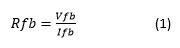
where Rfb = 1.25k.
Rfb1 sets the reference current for the current mirrors. Once again, with 1mA as the reference current and using Equation 2, calculate Rfb1 to set the output voltage:
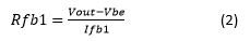
where VOUT = 12V, Rfb1 = 11.3k and Vbe is ~0.7V.
With 1mA flowing into Rfb2 and the emitter current being approximately equal to the collect current (Ie~Ic), this sets the reference current Iref2. The loop is closed and the voltage will regulate to the set voltage described.
Output Voltage Regulation
Example Schematic
/12VOUT At 3A Design Using the LM5085") Figure 6 A 24V to 150VIN (Max)/12VOUT At 3A Design Using the LM5085
Figure 6 A 24V to 150VIN (Max)/12VOUT At 3A Design Using the LM5085Figure 7 shows an efficiency plot taken from a prototype board, with efficiency (%) vs. load current (A).
 vs. Load Current (a) at Various Input Voltages") Figure 7 Efficiency (%) vs. Load Current (a) at Various Input Voltages
Figure 7 Efficiency (%) vs. Load Current (a) at Various Input VoltagesFigure 8 shows the switch-node voltage and inductor ripple current at 150VIN.
 Figure 8 Channel 1 Switch-node Voltage, Channel 4 Inductor Ripple Current