SSZTA69 may 2017 TPS7A3501
Let’s say that you are working on an ultrasound system. You require a clean ±100V supply to power the ultrasound transmitter, so you need a linear regulator (LDO). How do you tackle this requirement?

You could look for a device from a semiconductor manufacturer, but the chances of getting readily available voltage regulators (both positive and negative) that can support such high voltages are rare. You could create a discrete, old-fashioned, dissipative transistor-based regulator. Or you could use an existing off-the-shelf low-voltage regulator to fulfill your requirements by employing a trick called “floating.”
Floating has been around a long time. A floating regulator is a type of voltage regulator that works without a real ground connection. This is a trick used for regulating voltages higher than the regulator’s rated value. Many applications require circuit performances that are unachievable with conventional regulator designs. In this post, I’ll look at an innovative circuit that can float grounds for both positive and negative regulators. Although the examples shown are for voltage regulators, the circuits are applicable to power filters like the TPS7A3501 as well.
Floating Positive Regulator
TI’s TPS7A4701 is a 36V ultra-low noise (4μVRMS) LDO capable of sourcing a 1A load and providing a positive output voltage. External feedback resistors configure the TPS7A4701’s output voltage. To get the TPS7A4701 to support output voltages up to 100V, you can float the ground of the integrated circuit (IC) using a DC amplifier, as shown in Figure 1. In general, any positive regulator has some current flowing into the GND pin, which is listed as I(GND) in a data sheet. For the TPS7A4701, I(GND) is 6.1mA typical when the output current is 1A.
") Figure 1 DC Amplifier Simulation Using
TINA-TI™ Software for Floating Regulator Ground (Positive Regulator)
Figure 1 DC Amplifier Simulation Using
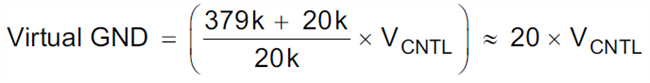
TINA-TI™ Software for Floating Regulator Ground (Positive Regulator)As shown in simulation in Figure 1, the LDO I(GND) is the current from the GND pin. This current is divided into two paths: one through a bipolar junction transistor (BJT) and the other through a resistor voltage divider. Operational amplifier (op amp) U1 operates as an integrator in an open-loop configuration and drives the BJT through a series resistance of 2.2 kΩ. A 12 V supply VCC supplies the op amp. The VCNTRL input decides the value of the virtual ground voltage, as shown in Equation 1.
The circuit shown in Figure 1 combined with the TPS7A4701 is tested during development for high-voltage operation. Figure 2 shows the transfer characteristics (for the circuit in Figure 1) with respect to the control voltage. The virtual ground is set using an external control voltage, VCNTL(P).
 Figure 2 Transfer Characteristics for a
Positive Regulator at an Input Voltage of 110V
Figure 2 Transfer Characteristics for a
Positive Regulator at an Input Voltage of 110VFloating Negative Regulator
The floating negative regulator example uses the TPS7A3301, a -36V ultra-low noise (16μVRMS, 72dB power supply rejection ratio [PSRR]) LDO capable of sinking a 1A load and providing a negative output voltage. For the TPS7A3301, I(GND) is specified as 5mA typical when the output current is 50mA. This current is diverted using a BJT, as shown in Figure 3.
") Figure 3 DC Amplifier Simulation Using TINA-TI™ Software for Floating Regulator Ground (Negative Regulator)
Figure 3 DC Amplifier Simulation Using TINA-TI™ Software for Floating Regulator Ground (Negative Regulator)Two op amps (U1 and U2) form a DC amplifier. The first stage converts the negative output voltage to a positive value. The second op amp is an error amplifier. The system has a stable point where the negative input becomes equal to the positive input of this second op amp. If the output goes too negative, the PNP transistor (at the output of the second op amp) is driven to saturation; this shifts the virtual ground toward zero. The VCNTL input decides the value of the output voltage by using Equation 2.
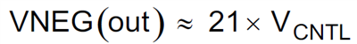
As shown in Figure 3, the output of the first op amp locks at the VCNTL voltage (= 1 V) and sets the negative output voltage at -21.32 V and virtual ground at -18.02 V.
The circuit shown in Figure 3 combined with the TPS7A3301 is tested during development for high-voltage operation. Figure 4 shows the transfer characteristics (for the circuit in Figure 3) with respect to the control voltage. The virtual ground is set using an external control voltage, VCNTL(N).
 Figure 4 Transfer Characteristics for a
Negative Regulator at an Input Voltage of -110 V
Figure 4 Transfer Characteristics for a
Negative Regulator at an Input Voltage of -110 VThe circuits used for floating the grounds are generic circuits. They use low-voltage op amps and external transistors to enhance the capability of existing low-voltage regulators.
Which techniques do you use for floating the ground? Tell us in the comments.
Additional Resources
- Jump-start your ultrasound power supplies with the new Programmable ±100-V, High-Current, Floating Linear Regulator Reference Design for Ultrasound Systems.
- Go through the application report for more such circuits: High Voltage Adjustable Power Supplies