SSZTAF8 february 2017 DLP4500 , DLP500YX , DLP6500FYE , DLP670S , DLPC350 , DLPC900
ADVANCE INFORMATION
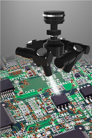
In my two decades with DLP Products, I’ve seen a wide variety of applications benefit from the use of DLP technology. The migration from 2D Automated Optical Inspection (AOI) to 3D AOI for printed circuit board manufacturing and inspection is no exception. The continuing miniaturization of consumer electronics offers new opportunities to improve inspection methods, like 3D AOI tactics, that can equate to manufacturing cost savings. If you are an AOI equipment designer, you may not know that you can leverage DLP solutions to help create the robust, high-speed, high resolution, high precision 3D imaging system necessary for successful inspection of PCB solder paste, solder joints, and accurate component placements.
The Need for 3D Inspection
3D AOI and Solder Paste Inspection (SPI) methods can help detect defects early in the assembly process, and combined with final inspection, help assure quality and reliability in the PCB manufacturing process with lower manufacturing costs.
As consumer electronics continue to reduce in size, it drives component sizes to shrink and PCB land geometries to increase in density. These properties may require additional 3D AOI or SPI capabilities to adequately assure final product quality.
3D AOI and SPI provide benefits at multiple stations in a PCB assembly factory including:
- Inline after solder paste application: Detection and correction of solder paste volume and shape deficiencies earlier in the line prevents expensive rework later.
- Inline after component placement: Verification of component installation and proper orientation helps prevent rework later.
- Inline at final inspection: Verifies all components are installed properly, components have not moved, component leads have not lifted, and all solder joints have proper amounts of solder, wicking without bridging, shorts, or opens.
- Offline inspection: Stand-alone unit to inspect reworked or manually assembled boards.
How Does 3D AOI Work?
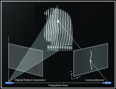
Many 3D AOI systems use DLP technology to quickly project up to 400 pre-determined patterns across a small field-of-view (FOV) on the target PCB. Monochrome or color cameras mounted to the side capture each projected pattern as it is deformed by the z-axis surface variation of the PCB components. The 3D shapes of the components are then derived through geometric triangulation analysis. The result is a 3D point cloud that a processor can compare to a reference model of “desired” physical attributes. The processor can then determine if any FOV contains attributes outside the expected norm, logs them as a fail condition, and provides the user the fail condition and location. Using this type of 3D structured light capability provides flexible, high precision 3D scanning to enable high speed inline inspection.
3D AOI Solutions Using DLP Technology
DLP technology brings many enhancements to AOI applications. For example, the DLP6500 digital micromirror device (DMD) is a 1920 x 1080 array of individually controlled mirrors which provides the high resolution, fast pattern rates, and programmability necessary for next generation 3D AOI applications. When coupled with the DLPC900 Controller, the two provide the following benefits:
- 8-bit phase shift pattern rates to nearly 250 patterns per second, enabling high speed data capture for incredibly fast PCB 3D AOI scan times.
- Programmable pattern selection and re-ordering ensure the “right” pattern gets applied to extract the most information for any FOV.
- DMD multi-wavelength support enabling multi-color AOI systems for optimized reflectivity and use with either monochrome or color cameras.
- Programmable pattern duration settings enable the software to control the “on-time” for each pattern to optimize the amount of light being reflected from the object.
- Triggers in and out allow the DLPC900 to trigger cameras for capture or to be triggered by cameras, processors, or other hardware.
DLP Products has a proven track record of MEMS technology leadership spanning more than 20 years. Multiple DMD resolutions and sizes support tiered AOI product positioning based on various scan speeds, resolutions, and price. In addition, our DLP Design Network provides expertise in designing and manufacturing solutions based on DLP technology in order to make product development easier and help customers accelerate their design process.
Related Resources
- Learn about machine vision technology using DLP technology
- Discover the TI Designs for High Resolution 3D scanner based on the DLP LightCrafter 6500 EVM and accurate point cloud generation for 3D machine vision applications using DLP Technology
- Ask your design questions to engineers on our E2E™ community