SSZTBZ2 November 2015 UCC27714
My previous blog post discussed isolation requirements in a typical power-supply system and two popular gate driver implementation methods: a gate drive transformer and a high-/low-side gate driver. A high-/low-side driver, such as the 600V UCC27714, can save over 50% in PCB layout area and much more on component volume.
In this post, I will discuss more details about the actual implementation of the two methods, including their strengths and weaknesses.
Figure 1 shows the actual implementation of a gate-drive transformer for a half-bridge MOSFET configuration. The additional components (compared to Figure 2a in my previous blog post) are necessary in order to have a clean and solid gate-drive signal on the MOSFETs. These additional components are:
- CB: a blocking capacitor to prevent gate drive transformer saturation.
- D1, D2: to prevent symmetrical negative-voltage bias and save gate drive loss.
- Q1, Q2: low-voltage P-MOSs or PNP transistor to enhance gate drive turnoff performance.
- Z1, Z2: Zener diodes to help protect the gate/source of the power MOSFET from overvoltage.
 Figure 1 Actual Implementation of a
Gate Drive Transformer, Considering Parasitics
Figure 1 Actual Implementation of a
Gate Drive Transformer, Considering ParasiticsObviously, additional components definitely increase gate drive transformer design complexity. Leakage inductances also hurt the performance of the gate drive transformer, including reduced peak gate drive current and large overshoot (caused by leakage inductance and MOSFET junction capacitances). Practically speaking,, increasing the peak-drive current necessitates increasing the core size and winding-wire thickness to facilitate higher driving speeds; the corresponding effect will be higher overshoot, however, since the leakage inductance stores higher energy. Bifilar winding of the gate-drive transformer could be helpful to minimize leakage inductance; however, the trade-off is increased primary-to-secondary winding coupled leakage capacitance, CIO. CIO is the one of the major parasitics that limits common-mode transient immunity (CMTI) performance (see my blog post, “48V systems: Driving power MOSFETS efficiently and robustly” for an explanation). In summary, it is really difficult to do a better trade-off given the above-mentioned factors.
Figure 2 shows the actual implementation of the high-side and low-side gate-driver solution with digital isolator. Compared to Figure 2b in my last post, I added only a few major components: RBoot and a 5V LDO, used to provide a power interface between VBias, 10 to 20V, and the isolator secondary side, which requires a 3 to 5V low voltage/power supply.
Because there is no transformer leakage inductance-related issue compared to a gate drive transformer, you can achieve better trade-offs among gate drive current, overshoot, CMTI, etc.
 Figure 2 Actual Implementation of
High-side and Low-side Gate Driver
Figure 2 Actual Implementation of
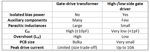
High-side and Low-side Gate DriverTable 1 compares the two methods. The high-/low-side gate driver does “win” from the perspective of having fewer auxiliary components, small parasitic inductances/CIO, smaller overshoot and PCB size, and flexible peak gate drive current. Concerning isolated bias power, as I mentioned before, the high-/low-side gate driver could take advantage of the existing offline isolated power-supply subsystem.
|
Stay tuned for the next installment of this series, when I will discuss the dynamic performance of each method.
Additional Resources
- Catch up with part one: Gate drive transformer vs. high/low side driver: Which way to go for power supply design?
- Check out TI’s new high-speed, 600V high-side low-side gate driver with 4A peak output.
- Design using the UCC27714