SSZTCA8 August 2015 LMV431
Current sources and sinks are essential components of analog design, from the simple biasing of active analog circuitry to current-capacitor integrator reset and oscillator architectures. A convenient topology for implementing current sources and sinks utilizes a field effect transistor (FET) driven by an operational amplifier to produce a current from the feedback of a small series resistance. Figure 1 depicts this topology.
 Figure 1 Feedback-generated Current
Source and Sink Circuits
Figure 1 Feedback-generated Current
Source and Sink CircuitsAs illustrated in Figure 1, both circuits use negative feedback to force a voltage across the RSET resistor, which generates the following source and sink currents (Equations 1 and 2):

For these currents to be available as DC, the numerator in Equations 1 and 2 above must be constant. The simplest way to achieve this is to use a shunt voltage reference, as shown in Figure 2.
 Figure 2 Feedback-generated Current
Source and Sink Circuits
Figure 2 Feedback-generated Current
Source and Sink CircuitsNote that in Figure 2, the RLIM resistor is used to drop excessive input voltage and limit current through the voltage reference. Further, a cathode-reference-tied adjustable voltage reference (such as the LMV431) forces the feedback voltage to its minimum value—this offers an important advantage that I’ll explore later. Equations 1 and 2 can now be rewritten as:

Equations 3 and 4 can be combined—since they are identical—and rewritten as Equation 5 to solve for the value of RSET required to produce an arbitrary source or sink current, ISET:

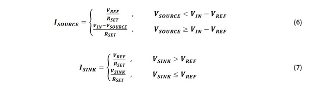
The output voltage range of this topology is limited by the headroom that must be maintained across the FET and RSET resistor. This is the reason for minimizing the forced feedback voltage—minimizing the forced feedback voltage maximizes the valid output voltage range. Equations 6 and 7 describe the current source and sink behavior inside and outside the valid output voltage region.
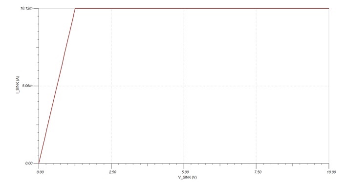
The internal VREF of any adjustable voltage reference is roughly 1.24V. Generated via bandgap reference, this specific voltage will ultimately define the limits of this topology overall. To demonstrate, Figure 3 is an example current sink characterization (including the linear current dropout) for an RSET value of 124Ω.
Substituting a bipolar junction transistor (BJT) for the FET in this topology may result in a marginally higher headroom requirement, although ultimately this substitution should behave almost identically.
The ideal current source is a fundamental element in circuit theory. While any physical implementation will always fall short of the ideal, it is valuable to understand the mechanisms behind these shortcomings so they can be mitigated or avoided. In the case of this topology, we have seen how the output voltage range impacts the output current and the important role that voltage reference selection plays in minimizing this.
Additional Resources
- Visit www.ti.com/vref for more information about TI’s voltage reference products.
- Download the “Voltage Reference Selection Basics” white paper for a detailed explanation of voltage reference selection with respect to analog-to-digital converter (ADC) resolution.
- Read the Open Systems article, “Shunt vs. series: How to select a voltage reference topology.”
- Read TI’s Precision Hub blog series, “Understanding Voltage References,” which discusses the applications of both shunt and series references and when to use them.
- Start your design in WEBENCH® Power Designer.