SSZTCH1 july 2015 CSD18531Q5A
Finally, we have arrived at the concluding entry in this "Understanding MOSFET Data Sheets" blog series attempting to demystify the power MOSFET data sheet. In this blog, we will take a look at some of the other miscellaneous switching parameters that appear in the MOSFET data sheet, and examine their relevance (or lack thereof) to overall device performance. Note that if you are more of a visual learner, you can watch the video "Understanding MOSFET data sheets - switching parameters".
On the one hand, switching parameters like output charge (QOSS) and the reverse recovery charge of the FET’s intrinsic body diode (Qrr) are crucial elements that are responsible for a great portion of the FET’s switching losses in many high frequency power supply applications. Sorry if it may be starting to sound like a broken record at this point, but designers need to be careful when comparing FETs based on these parameters, because as is so often the case, test conditions matter!
Figure 1 below shows the output charge and reverse recovery charge as two sides to the same coin, measured at two different rates of di/dt on TI’s CSD18531Q5A 60V MOSFET. On the left, Qrr was measured at 360A/µs to be 85nC, and on the right, it was measured at 2000A/µs to be 146nC. While there is no industry standard for di/dt to measure the part at, we have seen competitors rate all the way down to 100A/us, in order to give the appearance of extra low Qrr.
 Figure 1 Qrr And
QOSS Measured on the CSD18531Q5A At 360A/µs (Left) and 2000A/µs
(Right).
Figure 1 Qrr And
QOSS Measured on the CSD18531Q5A At 360A/µs (Left) and 2000A/µs
(Right).Qrr can have an even stronger dependence on the diode forward current (If) the test was conducted at. And even further complicating matters is that some vendors do not include QOSS as a separate parameter, but rather just absorb this into the specification of Qrr. Besides the test conditions listed on the data sheet, other considerations like parasitic board inductances and subjective measurement methodologies make it virtually impossible to compare these parameters from separate vendors’ data sheets. That is not to say they are not important parameters to consider and design around, but for reliable comparative data, the only effective solution is to collect it independently using a common methodology and board.
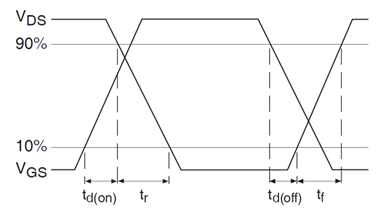
The last parameters I will mention in this series are switching times. These four parameters are defined generally by the waveform below in Figure 2 and appear on virtually every vendor’s data sheet. They are so dependent on board and test conditions that one veteran in the FET industry (and personal mentor) often cites these as “the most useless parameters on the FET data sheet.” Meant to give an indication of switching speed, the reality is these can be just as much a reflection of driver strength and drain current as they are the FET characteristics. TI includes these parameters as tested at the device’s rated current, while others will test these at only 1A ID, to give the appearance of a faster switching device. Much more indicative of the device’s actual switching speed are the gate charge parameters and the internal gate resistance of the device, Rg, both of which are significantly less susceptible to these specmanship games.
 Figure 2 Waveform Defining the MOSFET
Data Sheet Switching Times.
Figure 2 Waveform Defining the MOSFET
Data Sheet Switching Times.Thank you for taking the time to read this series on MOSFET data sheets. I hope you found this an enlightening read, and walk away with a more clear understanding of the value and ambiguities of the parameters that appear on the power MOSFET data sheet. Feel free to share the entire series with anyone who might benefit from this perspective on how to read a MOSFET data sheet. And don't forget to watch the video "NexFET™:Lowest Rdson 80 and 100V TO-220 MOSFETs in the World" and consider one of TI’s NexFET power MOSFET products for your next design.