SWRU620 April 2024
2.2.2 Switches
Table 3-2 shows the list of push buttons and usage.
Table 2-2 Switches Information
| Reference Designator | Usage | Comments | Image |
|---|---|---|---|
| SW1 | SOP0 | Switch between Functional and Flashing mode |
 Figure 2-3 SW1
Switch
 |
| S1.1 | SOP1 | OFF : Flashing / Functional Mode ON : Debug Mode |
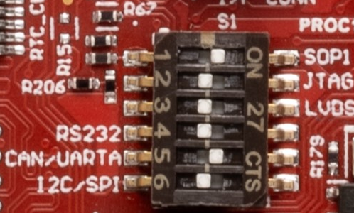 Figure 2-4 S1
Switch
 |
| S1.2 | JTAG | OFF : XDS_JTAG ON : DCA_JTAG |
|
| S1.3 | RDIF | OFF : RDIF ON : LIN_RX, XDS_UARTA/CAN, NERROR_LED, WATCH_DOG_TP, HOST_CLK_TP |
|
| S1.4 | RS232 | OFF : XDS_RS232 ON : DCA_RS232 |
|
| S1.5 | CAN/UARTA | OFF : CAN ON : XDS_UARTA |
|
| S1.6 | I2C/SPI | OFF : I2C, REG_MODE, LED_SW_GPIO ON : SPI |
|
| S4.1 | CAN Enable | OFF : CAN PHY : Stand-by Mode Disable ON : CAN PHY : Stand-by Mode Enable |
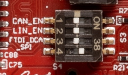 Figure 2-5 S4
Switch
 |
| S4.2 | LIN Enable | OFF : LIN PHY : Enable ON : LIN PHY : Disable |
|
| S4.3 | FTDI/DCA SPI | OFF : FTDI_SPI ON : DCA_SPI |
|
| S5.1 | XDS SDA | OFF : XDS_SDA Disable ON : XDS_SDA Enable |
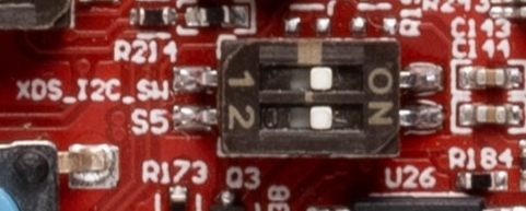 Figure 2-6 S5 Switch
 |
| S5.2 | XDS SCL | OFF : XDS_SCL Disable ON : XDS_SCL Enable |
|
| S2 | RESET Switch | Bounce Switch |
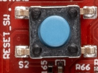 Figure 2-7 S2
Switch
 |
| S3 | USER Switch | Bounce Switch |
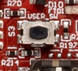 Figure 2-8 S3
Switch
 |
| SW2 | Reference Design Connectivity Switch | Switch between 5V and 3.3V : To
supply 5V to reference design (Only required when reference design is connected on EVM) |
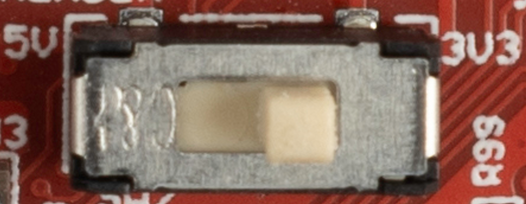 Figure 2-9 SW2 Switch
 |
| SW3 | Reference Design Connectivity Switch | OFF : Switch low to put reference
design into Flashing Mode (as shown in image) (Only required when reference design is connected on EVM) |
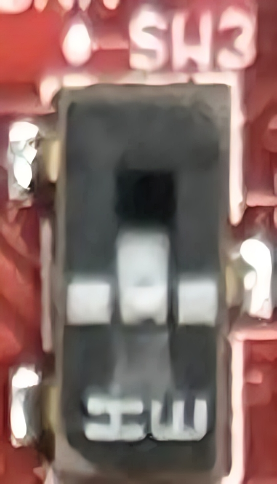 Figure 2-10 SW3 Switch
 |
Table 3-3 provides the list of LEDs and usage.
Table 2-3 LEDs Information
| Reference Designator | Color | Usage | Comments | Image |
|---|---|---|---|---|
| D3 | YELLOW | PGOOD | 3V3 supply indication | 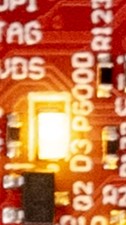 Figure 2-11 D3
 |
| D5 | GREEN | nRESET | This LED is used to indicate the state of nRESET pin. If this LED is glowing, then the device is out of reset. This LED glows only after the 5V supply is provided. | 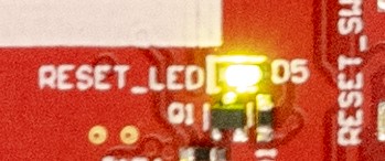 Figure 2-12 D5
 |
| D6 | GREEN | POWER | This LED indicates the presence of the 5V supply. |
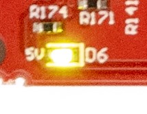 Figure 2-13 D6
 |
| D7 | GREEN | USER LED | Customer programmable user LED. Note: Switch S3 settings are needed to enable this. |
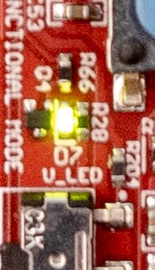 Figure 2-14 D7
 |
| D9 | RED | NERROUT | Glows if there is any HW error in the mmWave sensor device. |
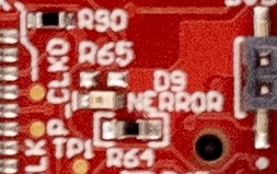 Figure 2-15 D9
 |
| D10 | YELLOW | FTDI | Glows if the USB is in suspend mode |
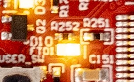 Figure 2-16 D10
 |