SWRZ092B April 2021 – March 2022 IWR6843AOP
- 1Introduction
- 2Device Nomenclature
- 3Device Markings
- 4Usage Notes
- 5Advisory to Silicon Variant / Revision Map
-
6Known Design Exceptions to Functional
Specifications
- MSS#03
- MSS#10
- MSS#11
- MSS#12
- MSS#13
- MSS#14
- MSS#16
- MSS#17
- MSS#18
- MSS#19
- MSS#20
- MSS#21
- MSS#22
- MSS#23
- MSS#24
- MSS#25
- MSS#26
- MSS#27
- MSS#28
- MSS#29
- MSS#30
- MSS#31
- MSS#32
- MSS#33
- MSS#34
- MSS#35
- MSS#36
- MSS#37B
- MSS#38A
- MSS#39
- MSS#40
- MSS#41
- MSS#42A
- MSS#43A
- MSS#44A
- MSS#45
- 6.1 MSS#50
- 6.2 MSS#51
- ANA#11B
- ANA#12A
- ANA#13B
- ANA#14
- ANA#16
- ANA#17A
- ANA#18B
- ANA#19
- ANA#20
- ANA#22A
- 6.3 ANA#27A
- ANA#30
- ANA#31
- DSS#01
- DSS#02
- DSS#03
- DSS#05
- DSS#07
- PACKAGE#01
- PACKAGE#02
- 7Trademarks
- 8Revision History
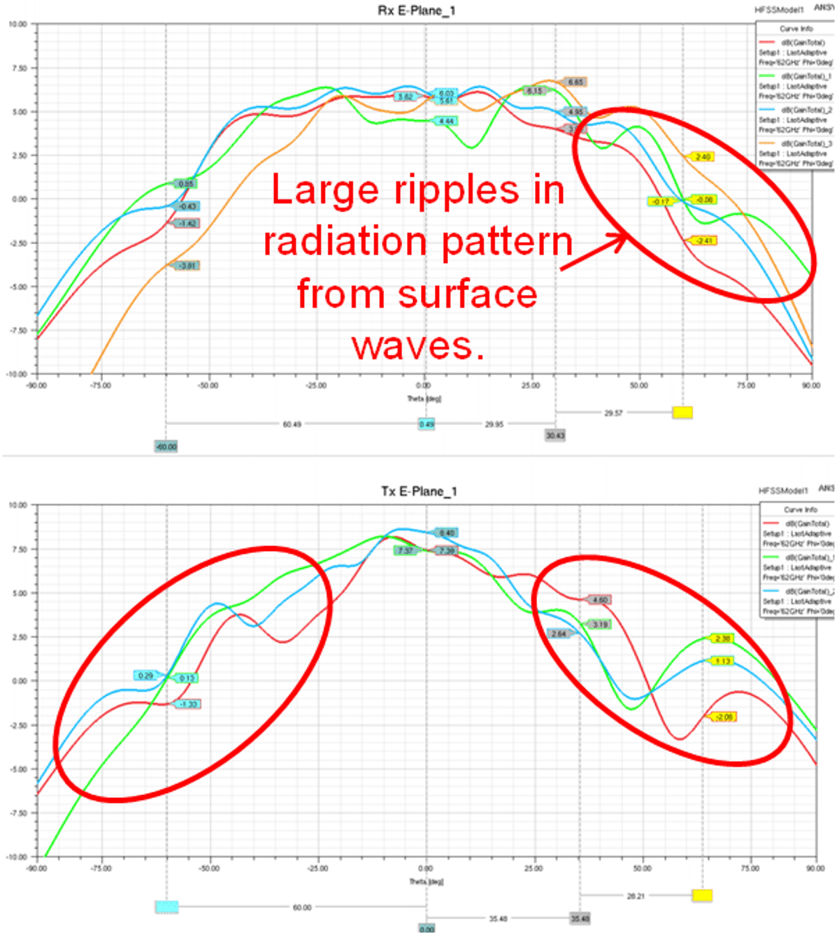
PACKAGE#02
Surface Wave Artifact from PCB
Revisions Affected
IWR6843AOP ES1.0 and IWR6843AOP ES2.0
Description:
Large PCBs area around the E-plane causes surface waves that create large ripples in the elevation direction of the AoP antenna radiation pattern.
Workaround #1
Keep the Edge of PCB close to the edge of the AoP device in the E-plane to minimize the surface wave ripples.
 Figure 6-5 Small form factor board with PCB edge less than 0.3mm
Workaround #2
If a larger board is needed for the solution, a trapezoid cutout with the PCB edge less than <0.3mm from the edge of the AoP should be implemented to minimize the ripples caused by surface waves.
 Figure 6-6 Large form factor board with trapezoidal cutout and PCB edge less than
0.3mm
Figure 6-6 Large form factor board with trapezoidal cutout and PCB edge less than
0.3mm