TIDT224 March 2021
4.1 Start-up Sequence
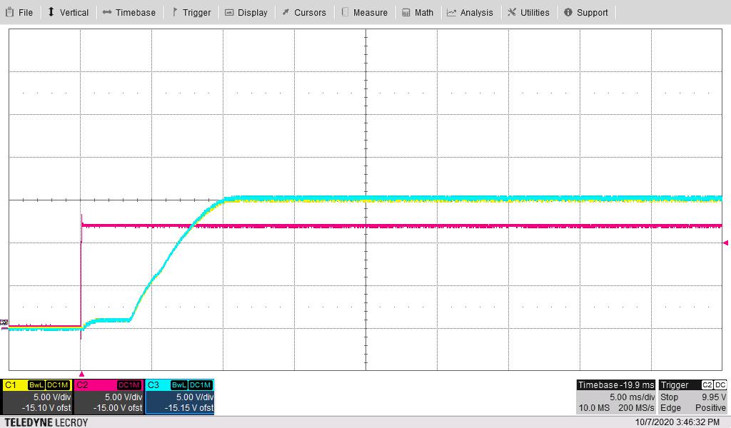
The following image shows the output voltage start-up waveforms (Vout1 in Blue, Vout2 in Yellow) after the application of 12-V input (Red) with each output loaded to 100 mA.

5 V/div, 5 ms/div
Figure 4-1 Output Voltage Start-up
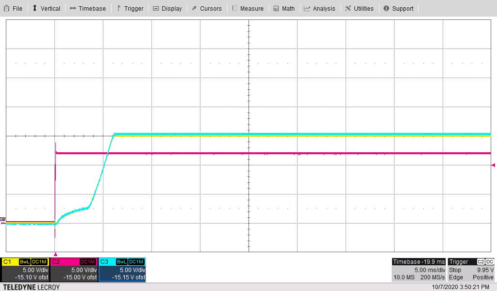
WaveformsThe following image shows the output voltage start-up waveforms (Vout1 in Blue, Vout2 in Yellow) after the application of 12-V input (Red) with each output loaded to 10 mA.

5 V/div, 5 ms/div
Figure 4-2 Output Voltage Start-up
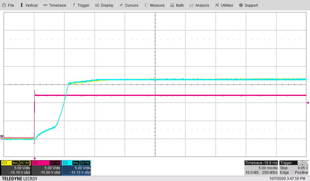
WaveformsThe following image shows the output voltage start-up waveforms (Vout1 in Blue, Vout2 in Yellow) after the application of 12-V input (Red) with each output loaded to 0 mA

5 V/div, 5 ms/div
Figure 4-3 Output Voltage Start-up
Waveform