TIDT226 April   2021


  1. 1Description
  2. 2Test Prerequisites
    1. 2.1 Voltage and Current Requirements
    2. 2.2 Required Equipment
  3. 3Testing and Results
    1. 3.1 Thermal Images
    2. 3.2 Efficiency and Power Dissipation Graph
    3. 3.3 Efficiency and Power Dissipation Data
    4. 3.4 Cross-Load Voltage Regulation
    5. 3.5 Voltage Regulation Graph
  4. 4Waveforms
    1. 4.1 Start-up Sequence
    2. 4.2 Switch Node
    3. 4.3 Output Voltage Ripple
    4. 4.4 Load Transients

Load Transients

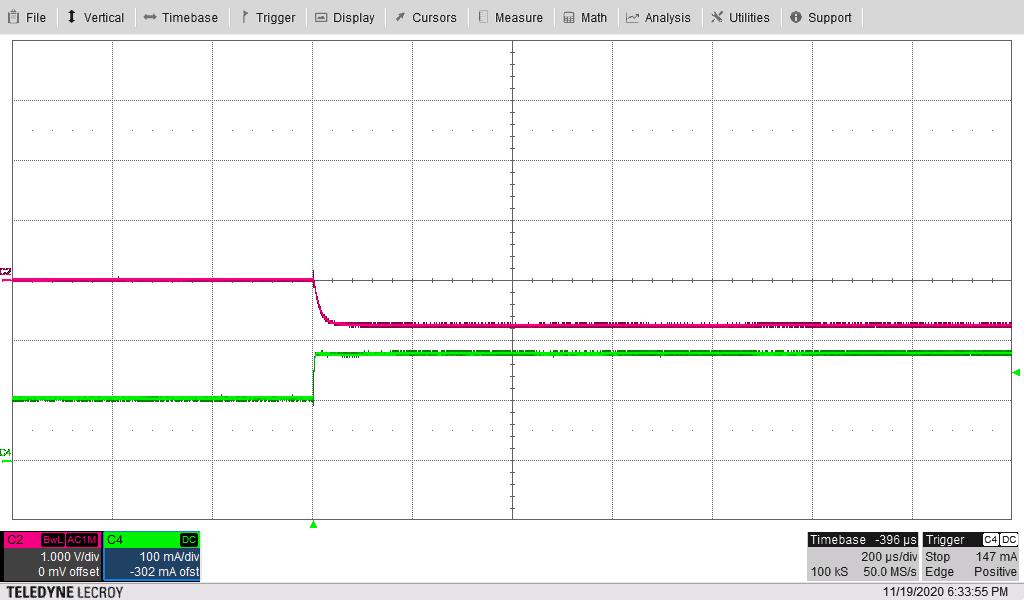
The total rectified secondary output voltage (AC coupled) is shown in Red in the following waveform for a load step (Green) from 100 mA to 175 mA with the input voltage at 24 V. The load current is sourced from the 20 V directly to the –4 V with no COM connection.
GUID-20210219-CA0I-59QM-VJDZ-T026MWHRVNVJ-low.jpg
1 V/div, 100 mA/div, 200 µs/div
Figure 4-15 Total Rectified Secondary Output Voltage (AC Coupled)

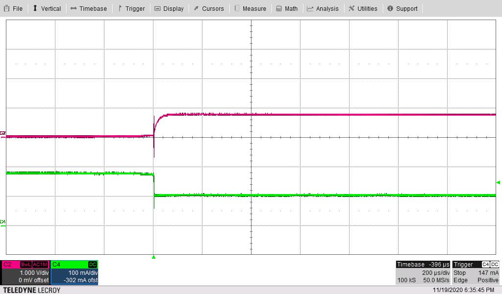
The total rectified secondary output voltage (AC coupled) is shown in Red in the following waveform for a load step (Green) from 175 mA to 100 mA with the input voltage at 24 V. The load current is sourced from the 20 V directly to the –4 V with no COM connection.
GUID-20210219-CA0I-BRMK-81RV-KSJQKTDSLFFX-low.jpg
1 V/div, 100 mA/div, 200 µs/div
Figure 4-16 Total Rectified Secondary Output Voltage (AC Coupled)