TIDT308 October   2022


  1.   Description
  2.   Features
  3.   Applications
  4. 1Test Prerequisites
    1. 1.1 Voltage and Current Requirements
    2. 1.2 Required Equipment
    3. 1.3 Considerations
    4. 1.4 Dimensions
    5. 1.5 Test Setup
  5. 2Testing and Results
    1. 2.1 Efficiency Graphs
    2. 2.2 Efficiency Data
    3. 2.3 Thermal Images
      1. 2.3.1 Top Side
      2. 2.3.2 Bottom Side
    4. 2.4 Bode Plots
  6. 3Waveforms
    1. 3.1 Switching
      1. 3.1.1 Secondary Side
      2. 3.1.2 Primary Side
        1. 3.1.2.1 Transistor Q8 Drain-Source
        2. 3.1.2.2 HS2-Pin of U1
          1. 3.1.2.2.1 Undershoot
          2. 3.1.2.2.2 Overshoot
    2. 3.2 Output Voltage Ripple
    3. 3.3 Load Transients
    4. 3.4 Start-Up Sequence
      1. 3.4.1 Full Load
      2. 3.4.2 Zero Load
      3. 3.4.3 Overload
    5. 3.5 Shutdown Sequence

Load Transients

The output voltage variation, during load transients, was measured by supplying the converter at 24 VDC and by switching the load current between 1.25 A and 2 A. For all waveforms, the bandwidth limit of the oscilloscope was set to 20 MHz
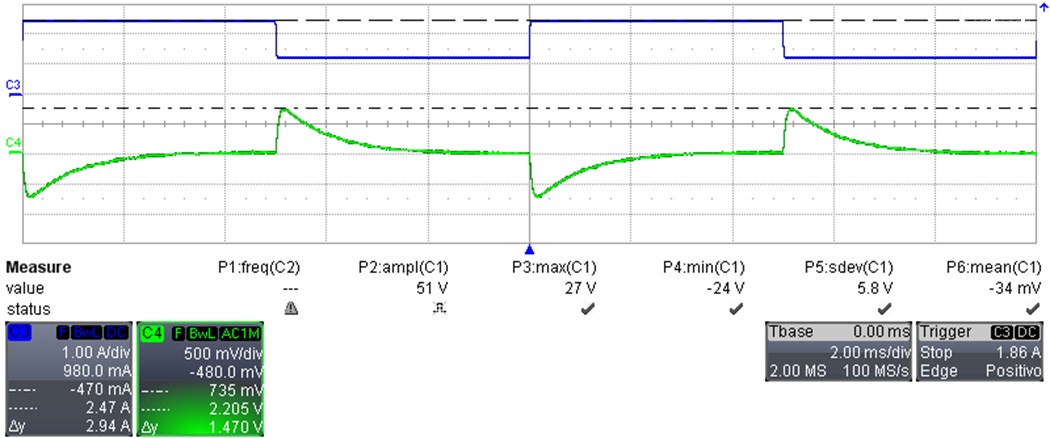
GUID-20220926-SS0I-VMNW-JKMF-B5BTP2LHCTBQ-low.png Figure 3-6 Load Transients 1.25 A to 2 A
  • Channel C4: Output voltage (500 mV / div, 2 ms / div, AC coupling)
  • Channel C3: Output current (1 A / div, DC coupling)