TIDUE53I march 2018 – july 2023 TMS320F28P550SJ , TMS320F28P559SJ-Q1
- 1
- Description
- Resources
- Features
- Applications
- 6
- 1System Description
- 2System Overview
-
3Hardware, Software, Testing Requirements, and Test Results
- 3.1 Required Hardware and Software
- 3.2 Testing and Results
- 4Design Files
- 5Trademarks
- 6About the Authors
- 7Revision History
3.2.2.2 Lab 3
In this lab the power stage is run in an closed loop on the real HW or HIL platform. Figure 3-10 shows the SW diagram.
 Figure 3-10 Lab 3 Software Diagram
Set the project to Lab 3 by changing the Lab Number in the <settings.h> file, (this will be changed by powerSUITE GUI when using powerSUITE project).
In the user settings.h file some additional options are available, but the following are used for the tests documented in this user guide.
#if TINV_LAB == 3
#define TINV_TEST_SETUP TINV_TEST_SETUP_RES_LOAD
#define TINV_PROTECTION TINV_PROTECTION_ENABLED
#define TINV_SFRA_TYPE TINV_SFRA_CURRENT
#define TINV_SFRA_AMPLITUDE (float32_t)TINV_SFRA_INJECTION_AMPLITUDE_LEVEL2
#define TINV_POWERFLOW_MODE TINV_INVERTER_MODE
#define TINV_DC_CHECK 0
#define TINV_SPLL_TYPE TINV_SPLL_DDSRF
#endif
Lab 3:
In this check, the SW is run on the hardware, or the HIL platform, or both.
Refer to the hardware test set up section for actual details of the equipment used for configuring the test. At this time, do not supply any HV power to the board.
- First launch the main.cfg and select lab3 in the project options. The compensator style (PI compensator) and the tuning loop (current loop) will be automatically populated. Now click run compensation designer icon and compensation designer tool will launch, with the model of the current loop plant with parameters specified on the powerSUITE page.
- The current compensator coefficients used for running the control loop are shown in the following code. The user can modify these coefficients to meet the necessary loop bandwidth and phase margin. The ideal coefficients with resistive load are slightly different than the one used for grid connection because the grid impedance is very low. The compensator design transfer function and response will be as shown in Figure 3-11.
#define TINV_GI_PI_KP ((float32_t)0.3)) #define TINV_GI_PI_KI ((float32_t)0.0120860479)) - Once satisfied with the proportional and integral gain values, click on Save COMP. This will save the compensator values into the project. Close the Compensation Designer, and return to the powerSUITE page
- Build and load the code, use the lab3.js file to populate the watch variables in the CCS window.
- Turn on the relay by writing a 1 to TINV_allRelaySet. The auxiliary power supply should draw close to 530 mA
- Set up an appropriate resistive load around 200 Ω to start with although the inverter mode can started at no load as well.
- Slowly ramp the DC bus voltage 'Vbus' to 800 V.
- Set the TINV_clearPWMTrip = 1, to clear the PWM trip signal. Now the switching action begins and sinusoidal voltages start appearing at the output. At this point the auxiliary power supply should draw close to 570 mA.
- As soon as TINV_clearPWMTrip is set, the TINV_closeGiLoop variable is enabled and closed current loop action begins.
- TINV_idRef_pu is the current command reference and by default it is populated to a value of 0.005 pu at start-up. Slowly vary this to increase the output AC voltage and observe measured current tracks the commanded value.
- Verify TINV_idRef_pu and TINV_iInv_dq0_pos.d data in the watch window at low before proceeding to close the current loop in Lab 3.
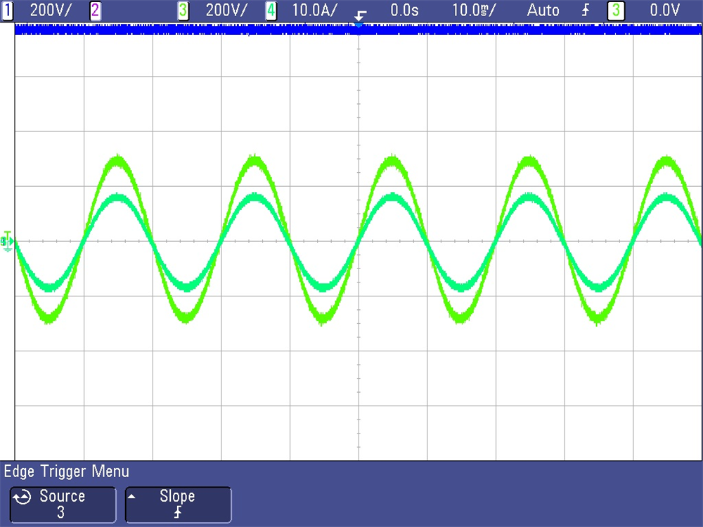
- Slowly increase id_ref to 0.36 pu at 800-V input voltage to improve output power to 3.7 kW, approximately 1.25 kW per phase. Figure 3-11 shows the power analyzer and scope waveform.
- Figure 3-11 shows the captured voltage and current waveform of inverter operating in closed current loop at 3.7 kW. Scope signals: Channel 1 - DC link voltage (blue), Channel 2 - AC voltage (light green), Channel 3 - AC current (dark green)
 Figure 3-11 Inverter Closed-Loop Operation
- SFRA is integrated in the software of this lab to verify the designed compensator provides enough gain and phase margin by measuring on hardware. To run the SFRA keep the project running, and from the cfg page, click on the SFRA icon. SFRA GUI will pop up.
- Select the options for the device on the SFRA GUI. For example, for F28377D select floating point. Click on Setup Connection. On the pop-up window uncheck the boot on connect option, and select an appropriate COM port. Click OK. Return to the SFRA GUI, and click Connect.
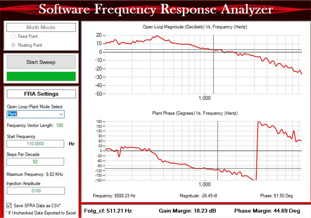
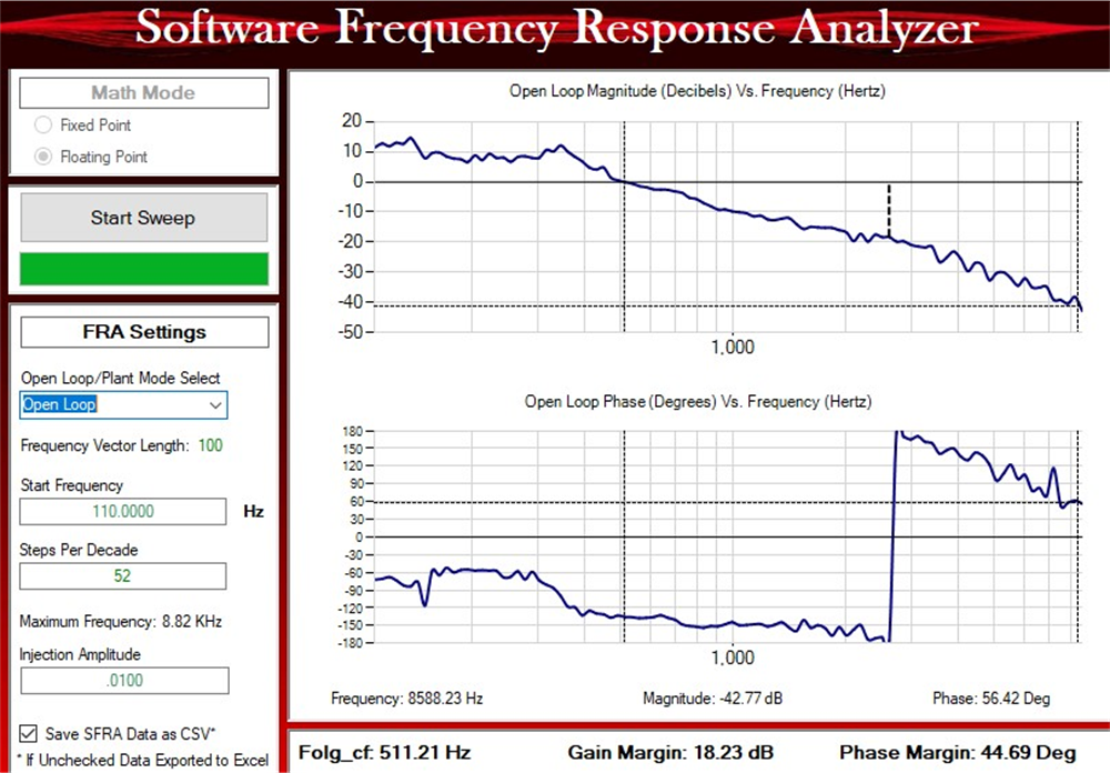
- The SFRA GUI will connect to the device. A SFRA sweep can now be started by clicking Start Sweep. The complete SFRA sweep will take a few minutes to finish. Activity can be monitored by seeing the progress bar on the SFRA GUI and also checking the flashing of blue LED on the back on the control card that indicates UART activity. Once complete, a graph with the open loop plot will appear, as in Figure 3-12. This verifies that the designed compensator is indeed stable. The SFRA for plant and open loop with the above coefficients is shown in Figure 3-12 and Figure 3-13, respectively. This action verifies the current compensator design. To bring the system to a safe stop, bring the input DC voltage down to zero.
- The above set of compensation designer coefficients are robust and stable. In case the tracking performance of current against the commanded reference and appears to oscillate, the user can use the following set of coefficients. To change the coefficients, compensation designer tool will have to be relaunched from the power suite page.
#define TINV_GI_PI_KP ((float32_t)0.144)) #define TINV_GI_PI_KI ((float32_t)0.112)) - Once satisfied with the proportional and integral gain values, click on Save COMP. This will save the compensator values into the project.
- The SFRA response of plant and open loop for the inverter in current mode with the new set of coefficients are shown in Figure 3-12 and Figure 3-13, respectively.
 Figure 3-12 Inverter SFRA Plant Response for Current Loop
 Figure 3-13 Inverter SFRA Loop Response for Current Loop