SBAU336A March 2020 – March 2021 AMC3306M05 , AMC3306M25 , AMC3336 , AMC3336-Q1
2.2 Digital Input and Output
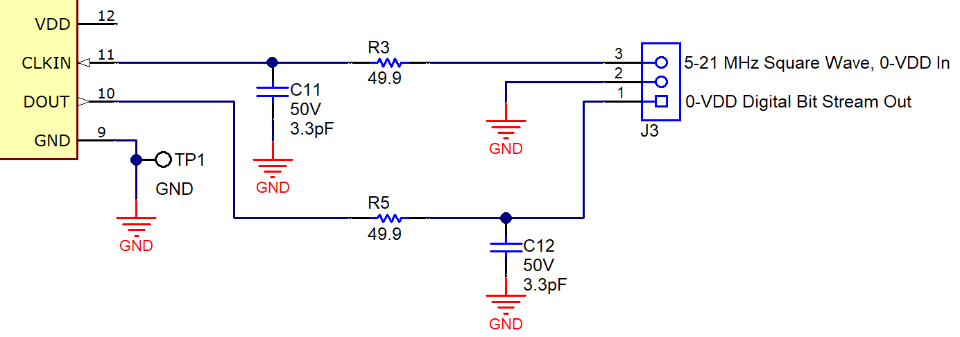
The digital CLKIN input for the AMC33xxEVM is accessible on the three-wire screw terminal at J3 on pin 3. The CLKIN input should be supplied with a 5–21 MHz square wave which alternates between 0 V and VDD.
The digital output from the AMC33xxEVM board is a bitstream with a ones density proportional to the differential input voltage. Figure 2-2 illustrates that the DOUT output is available at pin 1 of J3 .
 Figure 2-2 AMC33xxEVM Schematic: Digital Input and Output Section