SBOA181B February 2017 – November 2023 OPA2323 , OPA2325 , OPA2328 , OPA2388-Q1 , OPA320 , OPA322 , OPA323 , OPA363 , OPA364 , OPA365 , OPA369 , OPA388 , OPA388-Q1 , OPA4323 , TLV365
1
Introduction
Zero-crossover amplifiers use a unique topology which eliminates the error induced by the crossover region that standard rail-to-rail amplifiers have. TI’s zero-crossover topology assures high linearity across the entire common-mode voltage range and lowest distortion for precision and general applications. This application brief explains the differences between standard rail-to-rail input and zero-crossover amplifiers.
Traditional rail-to-rail CMOS input
A traditional rail-to-rail input CMOS architecture contains two differential pairs. Figure 1 highlights two differential pairs; one PMOS transistor pair (blue) and one NMOS transistor pair (red). PMOS transistors can operate in common-mode input voltages from VSS to (VDD-1.8 V) and NMOS transistors can operate in common-mode input voltages from (VDD-1.8 V) to VDD. The two input transistor pairs have independent and uncorrelated input offset voltages, temperature coefficients, and noise.
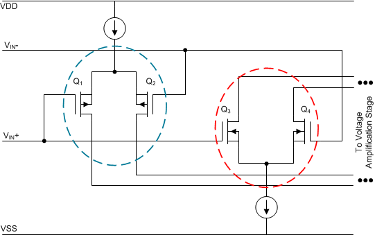 Figure 1 Simplified PMOS, NMOS
Differential Pair
Figure 1 Simplified PMOS, NMOS
Differential PairDuring the transition from the PMOS pair to the NMOS pair, and vice versa, there is a crossover region at approximately 1.8 V below the positive rail where both inputs are conducting (see Figure 2). Within this region, the DC input offset voltage can change. This is a source of distortion known as input crossover distortion. This offset error can be simulated using the TINA-TI SPICE tool.
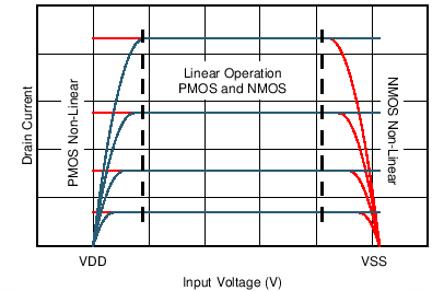 Figure 2 Transistor IV Curves
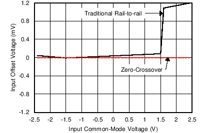 Figure 3 Simulated Crossover
Performance
Figure 3 Simulated Crossover
PerformanceFigure 3 shows the simulated results of applying a
[–2.4 V,
2.4 V] DC sweep to a traditional rail-to-rail CMOS input, buffer-configured op amp.
The graph shows the input offset voltage abruptly shifts when the common-mode
voltage is within the crossover region. If this error source is beyond the error
budget, a zero-crossover amplifier is required.
How zero-crossover works
Zero-crossover topology uses a internal voltage charge pump to achieve linear operation with input voltages up to the rail with a single input transistor pair (PMOS or NMOS). This use of a single transistor pair allows true rail-to-rail operation without distortion over the entire input common-mode range since there is no crossover region. Zero-crossover amplifiers such as the OPA388 include an internal voltage charge pump. The charge pump boosts the input stage voltage approximately 1.8 V above VDD. This is enough to overcome the non-linearity that occurs when the transistor enters triode operation at VDS < 1.8 V. Figure 4 shows a simplified representation of the charge pump topology used in zero-crossover amplifiers.
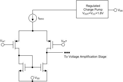 Figure 4 Simplified Zero-Crossover
Charge Pump Topology
Figure 4 Simplified Zero-Crossover
Charge Pump TopologyFigure 3 also shows the simulated results of applying a [–2.4 V, 2.4 V] DC sweep on a buffer-configured OPA388. The input offset voltage trace in the graph shows no abrupt shift with input common-mode change because there is no crossover region. Figure 5 contrasts the measured performance between a complementary rail-to-rail input and zero-crossover amplifier. Note the large variance in offset voltage across the input common-mode voltage.
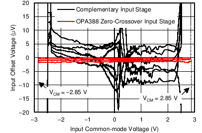 Figure 5 Measured Crossover
Performance
Figure 5 Measured Crossover
PerformanceZero-crossover vs. rail-to-rail CMOS results
A zero-crossover and a standard rail-to-rail CMOS amplifier were used in identical, unity-gain buffer configurations. These amplifiers were both fed a pure sine wave with an amplitude of 2 V (4 VPP). The outputs of these circuits were captured and the FFT was computed. Figure 6 shows the output voltage spectrum for the OPA388 (red) and a typical CMOS rail-to-rail amplifier (black). The output of the zero-crossover amplifier contains few spurs and harmonics compared to the typical rail-to-rail CMOS amplifier. This is the effect of eliminating the crossover region with zero-crossover topology.
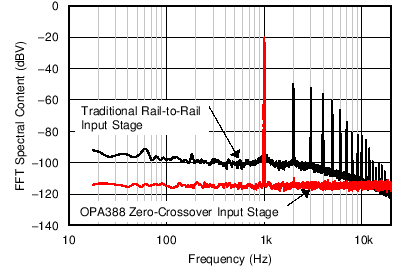 Figure 6 Buffer FFT Spectrum
Conclusion
Traditional rail-to-rail input CMOS op amps use two parallel differential input transistor pairs. When the common-mode is in the transition region (deadband), there is an abrupt shift in the input offset voltage which results in output voltage error and distortion. Zero-crossover op amps vastly reduce any changes in input offset voltage across the entire input common-mode range.
Additional Resources
Table 1 lists some of TI’s zero-crossover amplifiers. For a full list, see the operational amplifiers parametric search tool.
| Device | Optimized Parameters |
|---|---|
| OPA328 | Vos(max): 25 μV, GBW: 40 MHz, CMRR: 120 dB, IB(max): 1 pA, 2.2 V < VS < 5.5 V, Noise: 9.8 nV / √Hz |
| OPA323 | Vos(max): 1.25 mV, CMRR: 114 dB, GBW: 20 MHz, IB(max): 20 pA, Noise: 5.5 nV / √Hz, Slew Rate: 33 μV, 1.7 V < VS < 5.5 V |
| OPA388 | Zero-drift, Vos(max): 5 μV,
dvos/dt(max): 0.05 μV / °C, CMRR: 138 dB, GBW: 10 MHz, Noise: 7 nV / √Hz |
| OPA320 | Vos(max): 150 μV, CMRR: 114
dB, IB(max): 0.9 pA, GBW: 20 MHz, 1.8 V < VS < 5.5 V, Noise: 7 nV / √Hz |
| OPA325 | Vos(max): 150 μV, CMRR: 114
dB, IB(max): 10 pA, GBW: 10 MHz, 2.2 V < VS < 5.5 V, Noise: 9 nV / √Hz |
| OPA365 | Vos(max): 200 μV, CMRR: 120
dB, GBW: 50 MHz, Noise: 4.5 nV / √Hz, Slew rate: 25 V / μs, 1.8 V < VS < 5.5 V |
| OPA322 | Vos(max): 2 mV, CMRR: 100 dB,
GBW: 20 MHz, Noise: 8.5 nV / √Hz, Slew Rate: 10 V / µs, 1.8 V < VS < 5.5 V |
| OPA363,OPA364 | Vos(max): 2.5 mV, CMRR: 90
dB, GBW: 7 MHz, Noise: 17 nV / √Hz, IB(typ): 1 pA, 1.8 V < VS < 5.5 V |
| OPA369 | Vos(max): 750 µV, CMRR: 114
dB, GBW: 12 kHz, IB(typ): 10 pA, 1.8 V < VS < 5.5 V |