SBOA222A February 2018 – January 2019 LMV771 , LMV981-N
Design Goals
| Input | Output | Supply | ||||
|---|---|---|---|---|---|---|
| ViMin | ViMax | VoMin | VoMax | Vcc | Vee | Vref |
| –240 mV | 240 mV | 0.1 V | 4.9 V | 5 V | 0 V | 5 V |
Design Description
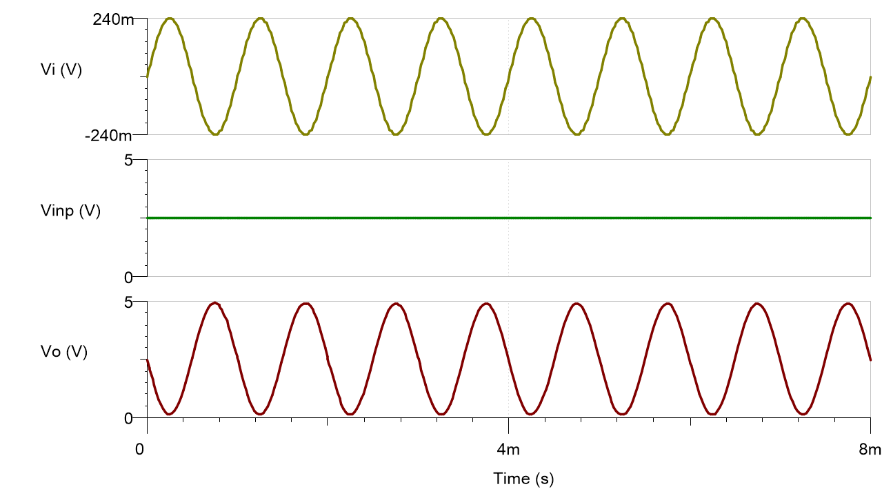
This circuit amplifies an AC signal and shifts the output signal so that it is centered at half the power supply voltage. Note that the input signal has zero DC offset so it swings above and below ground. The key benefit of this circuit is that it accepts signals which swing below ground even though the amplifier does not have a negative power supply.
Design Notes
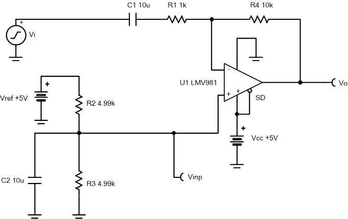
- R1 sets the AC input impedance. R4 loads the op amp output.
- Use low feedback resistances to reduce noise and minimize stability concerns.
- Set the output range based on linear output swing (see Aol specification).
- The cutoff frequency of the circuit is dependent on the gain bandwidth product (GBP) of the amplifier. Additional filtering can be accomplished by adding a capacitor in parallel to R4. Adding a capacitor in parallel with R4 will also improve stability of the circuit if high-value resistors are used.
Design Steps
- Select R1 and
R4 to set the AC voltage gain.
- Select R2 and
R3 to set the DC output voltage to 2.5 V.
- Choose a value for the lower cutoff
frequency, fl, then calculate C1.
- Choose a value for fdiv,
then calculate C2.
- The upper cutoff frequency,
fh, is set by the noise gain of this circuit and the gain
bandwidth (GBW) of the device (LMV981).
Design Simulations
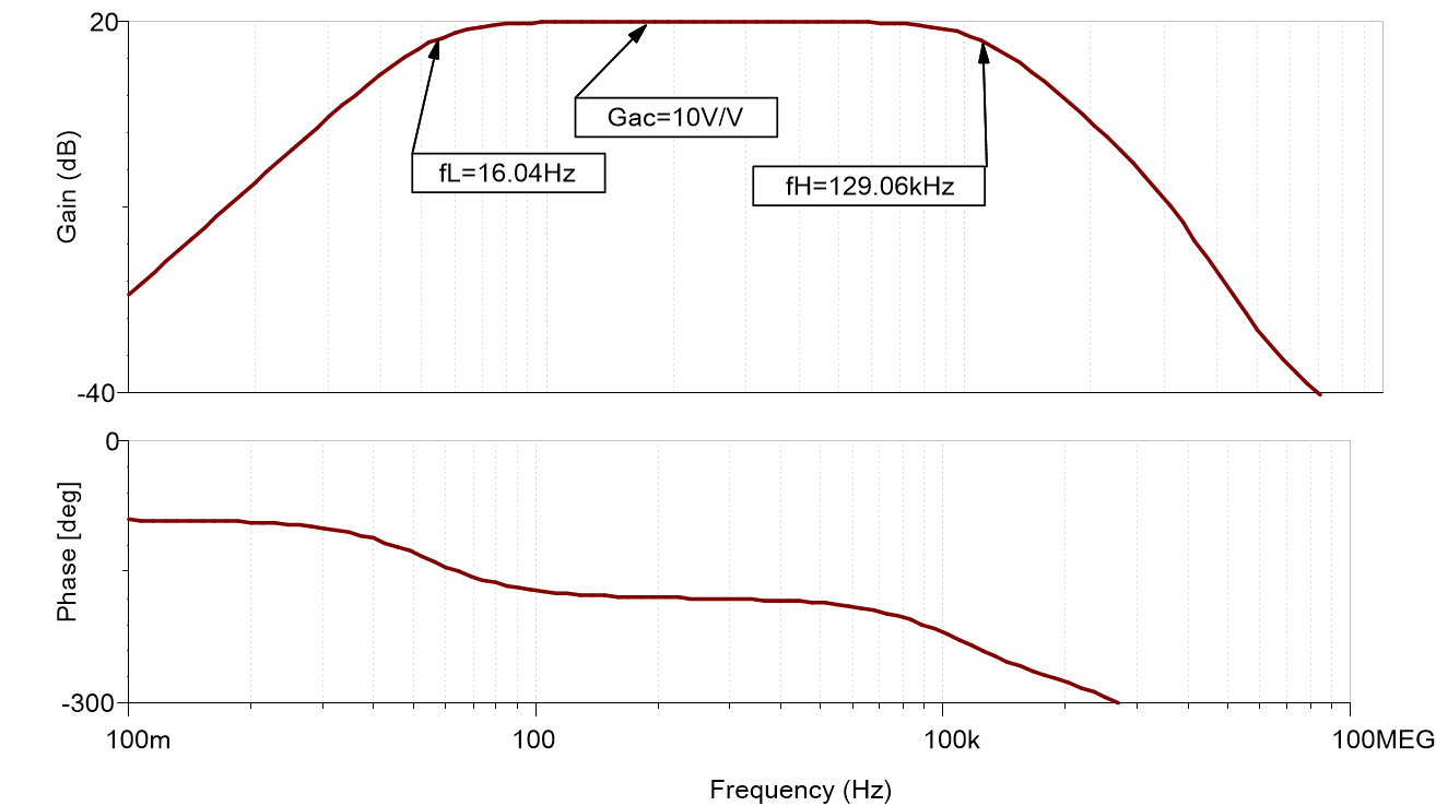
AC Simulation Results
Transient Simulation Results
Design References
See Analog Engineer's Circuit Cookbooks for TI's comprehensive circuit library.
See circuit SPICE simulation file SBOC504.
See TIPD185.
Design Featured Op Amp
| LMV981 | |
|---|---|
| Vcc | 1.8 V to 5 V |
| VinCM | Rail-to-rail |
| Vout | Rail-to-rail |
| Vos | 1 mV |
| Iq | 116 µA |
| Ib | 14 nA |
| UGBW | 1.5 MHz |
| SR | 0.42 V/µs |
| #Channels | 1 and 2 |
| LMV981 | |
Design Alternate Op Amp
| LMV771 | |
|---|---|
| Vcc | 2.7 V to 5 V |
| VinCM | Vee to (Vcc–0.9 V) |
| Vout | Rail-to-rail |
| Vos | 0.25 mV |
| Iq | 600 µA |
| Ib | –0.23 pA |
| UGBW | 3.5 MHz |
| SR | 1.5 V/µs |
| #Channels | 1 and 2 |
| LMV771 | |