SBOA233 January 2019 INA326 , OPA333
Design Goals
| Input | Output | Supply | Load Resistance (RL) | ||||
|---|---|---|---|---|---|---|---|
| ViMin | ViMax | ILMin | ILMax | Vcc | Vee | RLMin | RLMax |
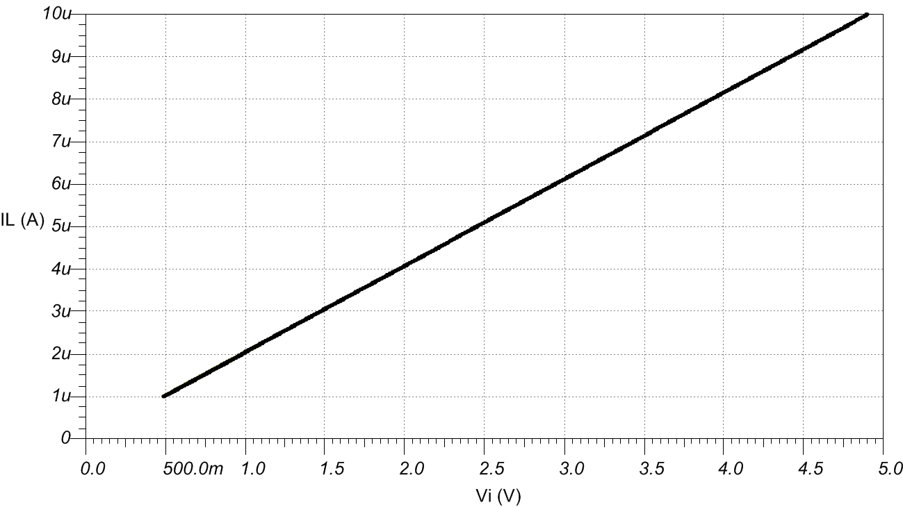
| 0.49 V | 4.9 V | 1 µA | 10 µA | 5 V | 0 V | 0 Ω | 390 kΩ |
Design Description
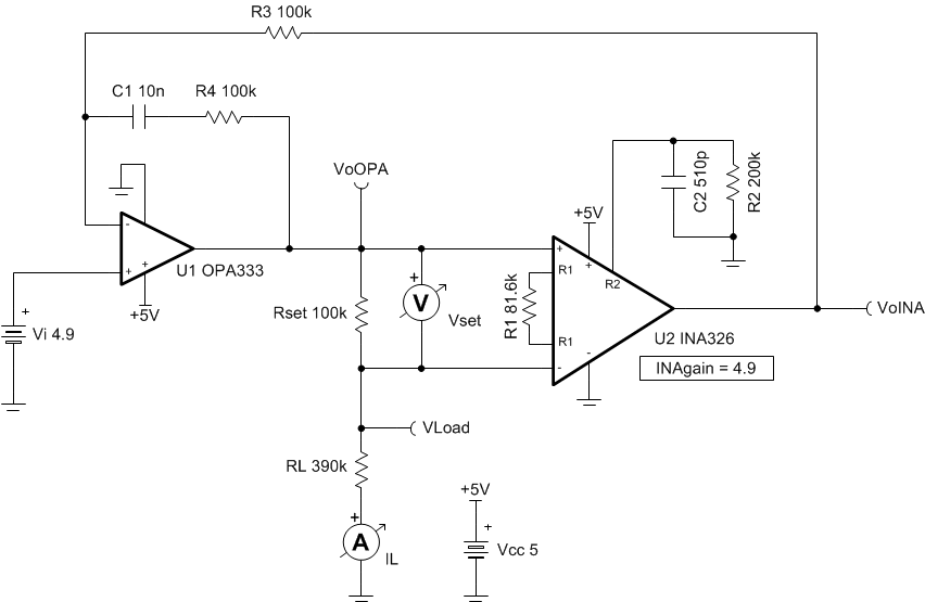
This circuit delivers a precise low-level current, IL, to a load, RL. The design operates on a single 5 V supply and uses one precision low-drift op amp and one instrumentation amplifier. Simple modifications can change the range and accuracy of the voltage-to-current (V-I) converter.
Design Notes
- Voltage compliance is dominated by op amp linear output swing (see data sheet AOL test conditions) and instrumentation amplifier linear output swing. See the Common-Mode Input Range Calculator for Instrumentation Amplifiers for more information.
- Voltage compliance, along with RLMin, RLMax, and Rset bound the IL range.
- Check op amp and instrumentation amplifier input common-mode voltage range.
- Stability analysis must be done to choose R4 and C1 for stable operation.
- Loop stability analysis to select R4 and C1 will be different for each design. The compensation shown is only valid for the resistive load ranges used in this design. Other types of loads, op amps, or instrumentation amplifiers, or both will require different compensation. See the Design References section for more op amp stability resources.
Design Steps
- Select Rset and check
ILMin based on voltage compliance.
- Compute instrumentation amplifier
gain, G.
- Choose R1 for INA326
instrumentation amplifier gain, G. Use data sheet recommended R2 =
200 kΩ and C2 = 510 pF.
- The final
transfer function of the circuit follows:
Design Simulations
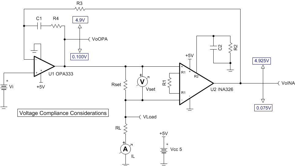
DC Simulation Results
| Vi | RL | IL | VoOPA | VoOPA Compliance | VoINA | VoINA Compliance |
|---|---|---|---|---|---|---|
| 0.49 V | 0 Ω | 0.999627 µA | 99.982723 mV | 100 mV to 4.9 V | 490.013346 mV | 75 mV to 4.925 V |
| 0.49 V | 390 kΩ | 0.999627 µA | 489.837228 mV | 100 mV to 4.9 V | 490.013233 mV | 75 mV to 4.925 V |
| 4.9 V | 0 Ω | 9.996034 µA | 999.623352 mV | 100 mV to 4.9 V | 4.900016 V | 75 mV to 4.925 V |
| 4.9 V | 390 kΩ | 9.996031 µA | 4.898075 V | 100 mV to 4.9 V | 4.900015 V | 75 mV to 4.925 V |
Design References
See Analog Engineer's Circuit Cookbooks for TI's comprehensive circuit library.
See the TINA-TI™ circuit simulation file, SBOMAT8.
See TIPD107.
See Solving Op Amp Stability Issues - E2E FAQ.
See TI Precision Labs - Op Amps.
Design Featured Op Amp
| OPA333 | |
|---|---|
| Vss | 1.8 V to 5.5 V |
| VinCM | Rail-to-rail |
| Vout | Rail-to-rail |
| Vos | 2 µV |
| Iq | 17 µA/Ch |
| Ib | 70 pA |
| UGBW | 350 kHz |
| SR | 0.16 V/µs |
| #Channels | 1 and 2 |
| OPA333 | |
Design Featured Instrumentation Amplifier
| INA326 | |
|---|---|
| Vss | 2.7 V to 5.5 V |
| VinCM | Rail-to-rail |
| Vout | Rail-to-rail |
| Vos | 20 µV |
| Iq | 2.4 mA |
| Ib | 0.2 nA |
| UGBW | 1 kHz (set by 1 kHz filter) |
| SR | 0.012 V/µs (set by 1 kHz filter) |
| #Channels | 1 |
| INA326 | |