SCDS371E January 2018 – April 2019 TS5MP646
PRODUCTION DATA.
- 1 Features
- 2 Applications
- 3 Description
- 4 Revision History
- 5 Pin Configuration and Functions
- 6 Specifications
- 7 Parameter Measurement Information
- 8 Detailed Description
- 9 Application and Implementation
- 10Power Supply Recommendations
- 11Layout
- 12Device and Documentation Support
- 13Mechanical, Packaging, and Orderable Information
7 Parameter Measurement Information
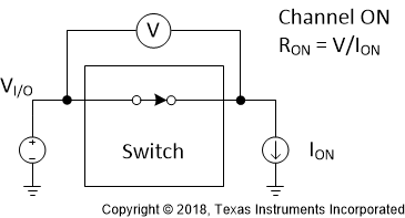 Figure 7. On Resistance
  Figure 8. Off Leakage
  Figure 9. On Leakage
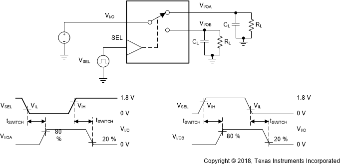
1. All input pulses are supplied by generators having the following characteristics: PRR ≤ 10 MHz, ZO = 50 Ω , tr = 3 ns, tf = 3 ns.
2. CL includes probe and jig capacitance.
Figure 10. tSWITCH Timing 
1. All input pulses are supplied by generators having the following characteristics: PRR ≤ 10 MHz, ZO = 50 Ω , tr = 3 ns, tf = 3 ns.
2. CL includes probe and jig capacitance.
Figure 11. tON and tOFF Timing for OE 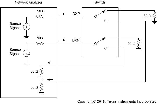 Figure 12. Off Isolation
 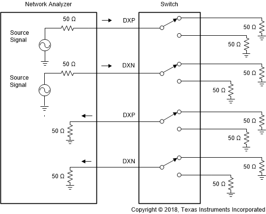 Figure 13. Crosstalk
 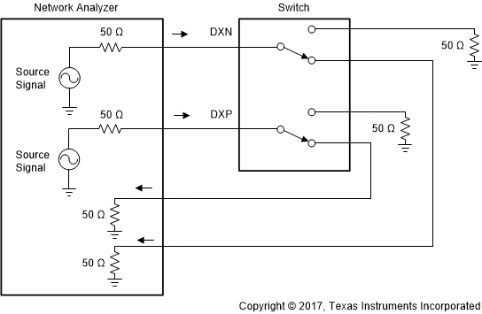 Figure 14. Bandwidth and Insertion Loss
 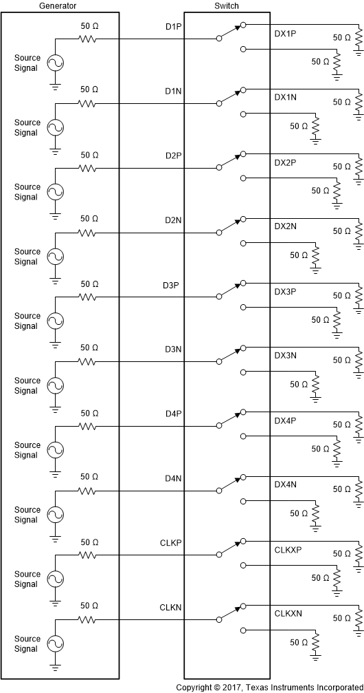 Figure 15. tPD, tSKEW(INTRA) and tSKEW(INTER) Setup
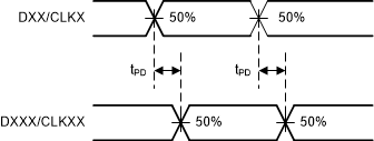
1. All input pulses are supplied by generators having the following characteristics: PRR ≤ 10 MHz, ZO = 50 Ω , tr = 100 ps, tf = 100 ps.
2. CL includes probe and jig capacitance.
Figure 16. tPD 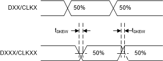
1. All input pulses are supplied by generators having the following characteristics: PRR ≤ 10 MHz, ZO = 50 Ω , tr = 100 ps, tf = 100 ps.
2. CL includes probe and jig capacitance.
Figure 17. tSKEW(INTRA) 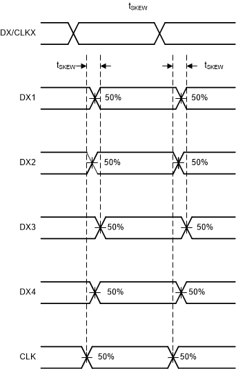
1. All input pulses are supplied by generators having the following characteristics: PRR ≤ 10 MHz, ZO = 50 Ω , tr = 100 ps, tf = 100 ps.
2. CL includes probe and jig capacitance.
3. tSKEW is the max skew between all channels. Diagram exaggerates tSKEW to show measurement technique
Figure 18. tSKEW(INTER) 
1. All input pulses are supplied by generators having the following characteristics: PRR ≤ 10 MHz, ZO = 50 Ω , tr = 3 ns, tf = 3 ns.
2. CL includes probe and jig capacitance.
Figure 19. tBBM