SCPA063 March 2023 PCA9306
3.2 Setting up the Oscilloscope
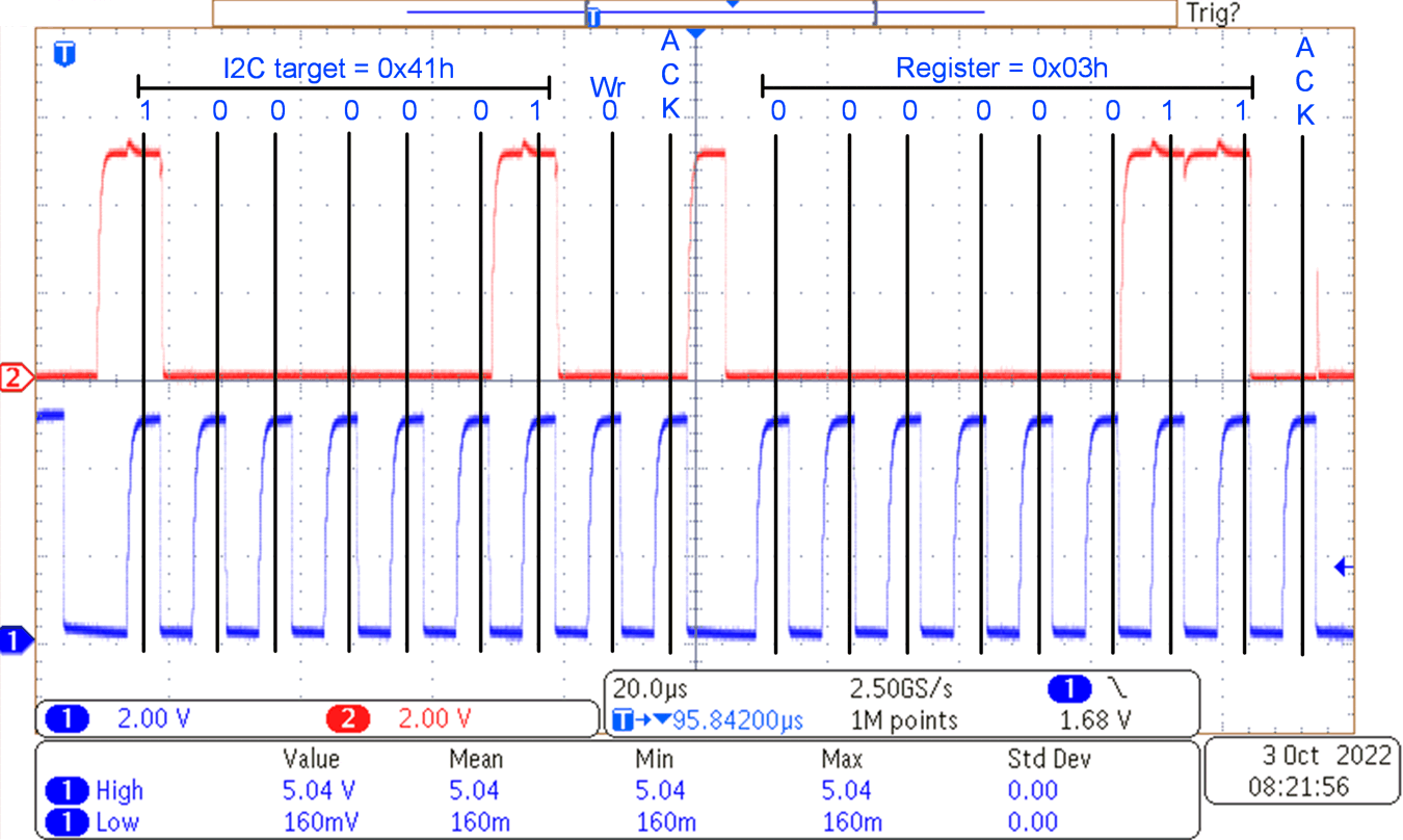
Use an oscilloscope to view entire frames of transferred data when debugging an I2C bus. Adjust the y-axis of an oscilloscope window such that the entire voltage range of the measured SDA and SCL signals are both viewable within the same scope window. Set up the x-axis of the oscilloscope window so that the following is clearly visible: the start condition, stop condition, and all address and data bits of a single frame. If possible, place the measured SDA and SCL signals directly on top of each other with a voltage offset in the oscilloscope window (doing this makes verifying the individual data bits easier to match to their corresponding clock pulses). Figure 3-1 shows an example of how an oscilloscope window screenshot looks.
 Figure 3-1 Example of a Debugging Scope Shot by Looking at the Data While the Clock Period is a Logic High