SLLA334B August 2018 – September 2022 ISO1050 , SN6501
3.2 5-V to 5-V Isolated Power Design Consideration
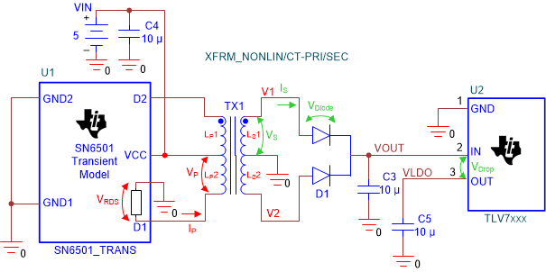
Figure 3-3 is the reference schematic for 5-V to 5-V isolated power supply.
 Figure 3-3 Reference Design for 5-V to 5-V Isolated
Power Supply (Pspice Schematic)
Figure 3-3 Reference Design for 5-V to 5-V Isolated
Power Supply (Pspice Schematic)SN6501 provides low ripple on rectified output. The linear regulator may not be used when the primary side of the transformer is supplied with a stable 5-V power (VIN). However, especially in a safety-related application, such as distributed control systems (DCSs), the programmable logic controller (PLC) and textile machinery controller, ±10% tolerance of VIN should be considered. So, 5-V power supply varies from 4.5 to 5.5 V and output of rectifier (VOUT) also varies with the same ratio. While the power supply at the secondary side (VLDO) of ISO1050 allows only 4.75 to 5.25 V, a 5-V LDO is needed to stabilize the output of the rectifier.
The two main factors to select an LDO are current drive capacity and input voltage range. SN6501 only provides current for ISO1050, thus the current drive capability depends on ISO1050 and should have headroom for the maximum current. For 80 mA (maximum) loading of ISO1050, a 100- to 150-mA LDO, such as TPS70950 or TLV70450, is appropriate.
The transformer output voltage range depends on transformer turns ratio. Minimum VIN and LDO efficiency should be considered to determine the turn ratio. Larger ratio can avoid the LDO step into nonlinear region when VIN drops (VOUT drops accordingly) and maintains a stable 5-V output. However, this results in low efficiency due to a larger drop in voltage on the LDO, and also forces the LDO input voltage to exceed the rating when VIN increases drastically.
Based on the power conservation principle for the transformer,
Also, according to the same volume of magnetic flux, which flows through the transformer primary and secondary coils, we have:
- VP = VIN - VRDS and is the voltage at the transformer primary side.
- VS = VLDO + VDiode + VDrop and is the voltage at the secondary side.
- VRDS is the drop voltage on the turnon resistor of the SN6501 power transistors, which varies with the changing of the loading current.
- VDiode is the diode forward voltage.
- VDrop is the LDO drop voltage.
Assume ISO1050 with the maximum loading, LDO must provide 80 mA current (IS-max).
To solve this linear equation of two unknowns (n and IP) under below condition: VLDO = 5 V, VDiode = 0.2 V, RDS = 2 Ω (at 5 V). Normally, although a voltage drop of LDO is around 150 mV at 100-mA loading, some low cost LDO has a larger drop voltage. For a worst case, consider VDrop-max = 1 V (at 100 mA). Gets n = 1.25, IP = 100 mA.
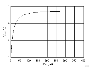
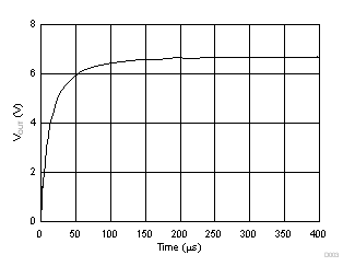
According to the preceding theoretical calculation, if ISO1050 is under the maximum current load, LDO must provide about 80 mA current with a 1-V drop. Turn ratio of transformer should not be less than 1.25. Meanwhile, the maximum primary current provided by SN6501 is 100 mA (IP) which is within the range of 350 mA at 5-V power supply. Figure 3-4 and Figure 3-5 show the Pspice simulation when input voltage drops or increases to the design limitation. Based on the simulation and calculation, the minimum transformer output is 5.45 V; thus, it is important to select an LDO with a drop voltage of less than 450 mV at 100 mA maximum loading.

| VOUT = 5.45 V |

| VOUT = 6.7 V |