SLLSF27D November 2018 – June 2022 TLIN1441-Q1
PRODUCTION DATA
- 1 Features
- 2 Applications
- 3 Description
- 4 Revision History
- 5 Description (continued)
- 6 Pin Configuration and Functions
- 7 Specifications
- 8 Parameter Measurement Information
-
9 Detailed Description
- 9.1 Overview
- 9.2 Functional Block Diagram
- 9.3
Feature Description
- 9.3.1 LIN Pin
- 9.3.2 TXD (Transmit Input)
- 9.3.3 RXD (Receive Output)
- 9.3.4 WAKE (High Voltage Local Wake Up Input)
- 9.3.5 WDT/CLK (Pin Programmable Watchdog Delay Input/SPI Clock)
- 9.3.6 WDI/SDI (Watchdog Timer Input/SPI Serial Data In)
- 9.3.7 PIN/nCS (Pin Watchdog Select/SPI Chip Select)
- 9.3.8 LIMP (LIMP Home output – High Voltage Open Drain Output)
- 9.3.9 nWDR/SDO (Watchdog Timeout Reset Output/SPI Serial Data Out)
- 9.3.10 VSUP (Supply Voltage)
- 9.3.11 GND (Ground)
- 9.3.12 EN/nINT (Enable Input/Interrupt Output in SPI Mode)
- 9.3.13 nRST/nWDR (Reset Output/Watchdog Timeout Reset Output)
- 9.3.14 VCC (Supply Output)
- 9.3.15 Protection Features
- 9.4 Device Functional Modes
- 9.5 Programming
- 9.6 Registers
- 10Application and Implementation
- 11Power Supply Recommendations
- 12Layout
- 13Device and Documentation Support
- 14Mechanical, Packaging, and Orderable Information
9.4 Device Functional Modes
nRST: Float
nRST: Float
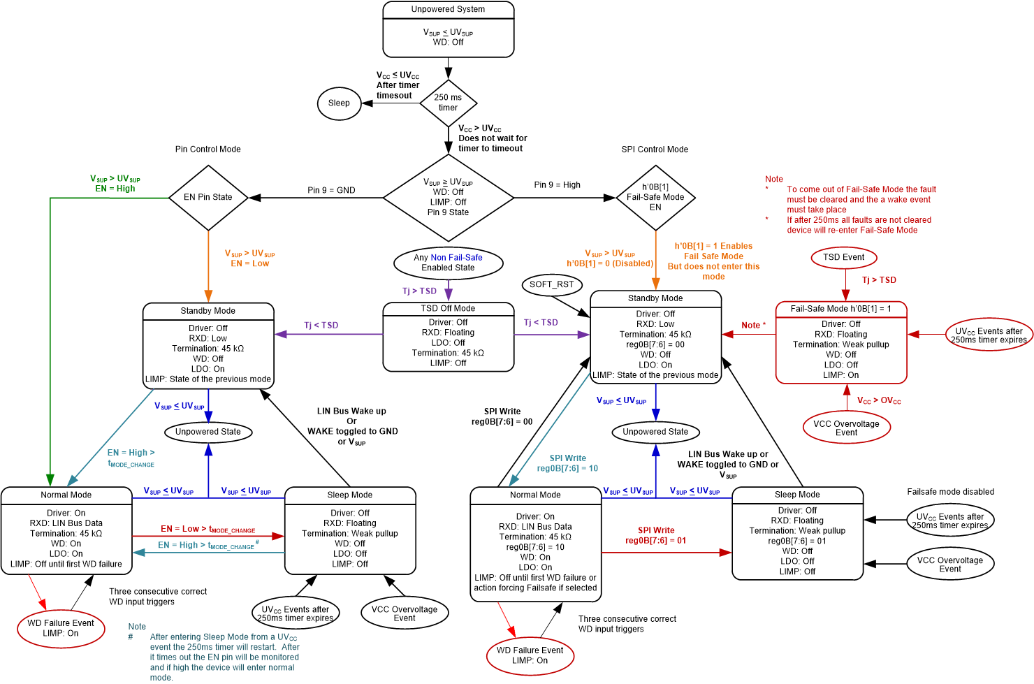
The TLIN1441-Q1 has three functional modes of operation: normal, sleep, and standby. The next sections describes these modes as well as how the device moves between the different modes. Figure 9-7 graphically shows the relationship while Table 9-1 shows the state of pins.
Table 9-1 Operating SPI Mode
| Mode | RXD | LIN BUS Termination | Transmitter | Watchdog | SPI Pins | nINT Pin | nRST/ nWDR Pin | WAKE Pin | LIMP | Comment |
|---|---|---|---|---|---|---|---|---|---|---|
| Sleep | Floating | Weak current pull-up | Off | Off | Off | On | Floating | On | Off | nRST is internally connected to the LDO output which in sleep mode is off |
| Standby | Low | 45 kΩ (typical) | Off | Off | On | On | On | On | Previous state prior to entering STBY | wake-up event detected, waiting on processors to set EN |
| Normal | LIN Bus Data | 45 kΩ (typical) | On | On | On | On | On | On | Off but can be active | LIN transmission up to 20 kbps |
| TSD Off | NA | Floating | 45 kΩ (typical) | Off | On | On | Floating | On | Off | nRST is floating but if OVCC is reached this value may show up on nRST pin |
| Failsafe | Floating | Weak current pull-up | Off | Off | Off | On | Floating | On | On | Failsafe mode is sleep mode with LIMP on |
Table 9-2 Operating PIN Mode
| Mode | EN | RXD | LIN BUS Termination | Transmitter | Watchdog | nRST Pin | WAKE Pin | LIMP | Comment |
|---|---|---|---|---|---|---|---|---|---|
| Sleep | Low | Floating | Weak current pull-up | Off | Off | Floating | On | Off | nRST is internally connected to the LDO output which in sleep mode is off |
| Standby | Low | Low | 45 kΩ (typical) | Off | Off | On | On | Previous state prior to entering STBY | Wake-up event detected, waiting on processors to set EN |
| Normal | High | LIN Bus Data | 45 kΩ (typical) | On | On | On | On | Off but can be active | LIN transmission up to 20 kbps |
| TSD Off | NA | Floating | 45 kΩ (typical) | Off | Off | Floating | On | Off | nRST is floating but if OVCC is reached this value may show up on nRST pin |
 Figure 9-7 State Diagram with Failsafe