SLLU322A September 2020 – October 2022 ISO1640
6 EVM Schematic and PCB
The ISO1640 isolated I2C EVM comes with an ISO1640D installed in place of U1. This EVM can also be configured for use with an ISO1641D, ISO1640DW, or ISO1641DW.
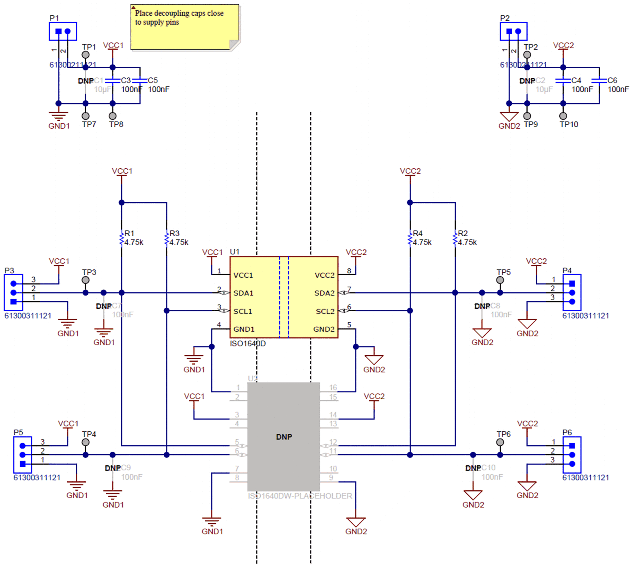
Each signal line (SDAx, SCLx) is configured with a 4.75-kΩ pull-up resistor (R1 to R4) to the corresponding power supply (Vccx). These resistors may be replaced with 0805 resistors of other values per the application requirements; for insight on calculating approprate pull-up resistor values for I2C buses, please refer to SLVA689, I2C Bus Pullup Resistor Calculation.
Signal pins my be tied directly to ground using the ground jumpers (P3 and P5 on side 1; P4 and P6 on side 2) to simulate a device pulling the I2C line low. While not being actively driven low, the lines will be pulled up through the included pull-up resistors. Signal lines should not be tied directly to a supply voltage without a pull-up resistor to limit input current. These jumpers also provide input /output signal access, including for oscilloscope probes, to each pin.
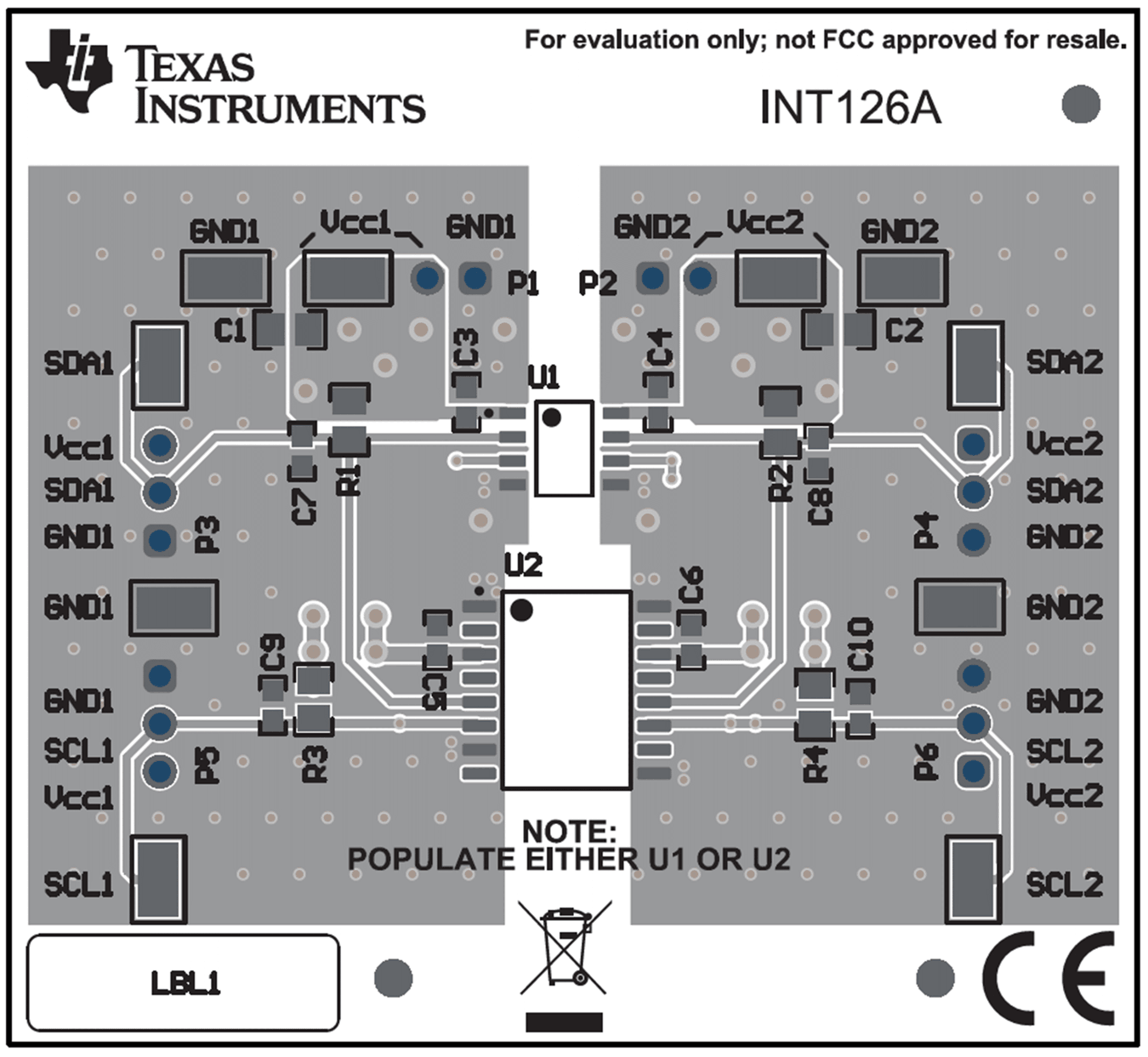
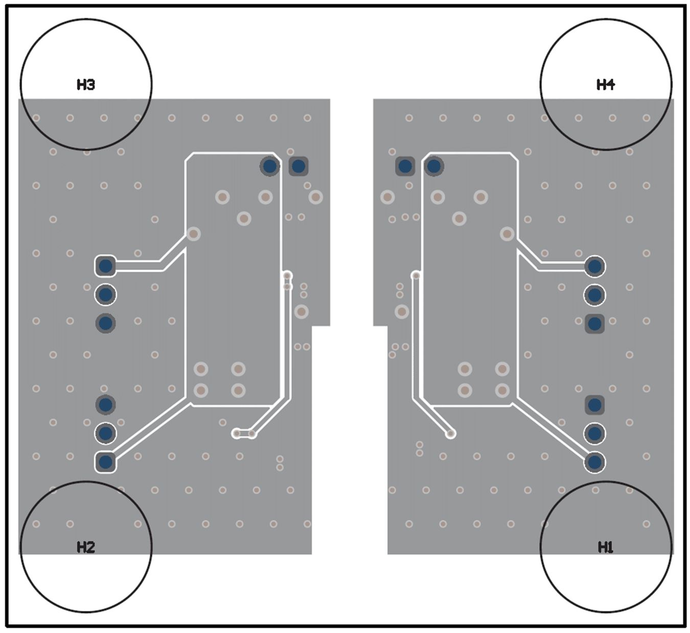
A schematic diagram for this EVM is shown in Figure 6-1 below, and Figure 6-2 and Figure 6-3 show the printed circuit board (PCB) layout.

Figure 6-1 ISO1640DEVM Schematic
 Figure 6-2 ISO1640DEVM Top PCB Layout
 Figure 6-3 ISO1640DEVM Bottom PCB Layout