SLOA284A january 2020 – may 2023 AFE5832 , AFE5832LP , ISO7741 , ISOW7841 , LM25037 , LM25180 , LM5180 , LM5181 , LM5181-Q1 , TX7316 , TX7332
4.1 Option 1: Programmable Output Voltage
Based on the various ultrasound operating modes, the output of the high voltage circuit should be programmable. This can be implemented as shown in Figure 2-2 by replacing the diode D18 with one resistor R3, joining the feedback resistors (shown in Figure 4-1). Output voltage can be varied through the control voltage (VDAC). Resistors can be set using equations (2), (3), (4) where R1 and R2 are the feedback resistors.
 Figure 4-1 Implementation of Programmable Output
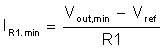
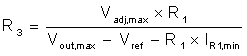
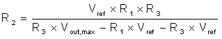
Figure 4-2 shows linear relationship between the programmed output voltage and the control voltage.
") Figure 4-2 Linearity of Output Voltage vs Control Voltage (VDAC)
Figure 4-2 Linearity of Output Voltage vs Control Voltage (VDAC)The designer should take care of the saturation current rating of the secondary inductors to take care of increased output current at reduced output voltage. In SEPIC converter the current is provided mainly from secondary inductors during off time. In this design, the secondary inductors are rated for 80 mA.