SLUU274A May 2007 – January 2022 TPS40193
- Trademarks
- 1Introduction
- 2TPS40193EVM-001 Electrical Performance Specifications
- 3Schematic
- 4General Configuration and Description
- 5Test Setup
- 6TPS40193EVM-001 Typical Performance Data and Characteristic Curves
- 7EVM Assembly Drawings and Layout
- 8Bill of Materials
- 9Revision History
7 EVM Assembly Drawings and Layout
Figure 7-1 through Figure 7-6 show the design of the TPS40193EVM-001 printed circuit board (PCB). The EVM has been designed using a 4-layer, 2oz, copper-clad PCB (2.5 inch × 2.5 inch), with all components in a 1.54-inch × 0.76-inch active area on the top side and all active traces to the top and bottom layers of the board. This configuration allows the user to easily view, probe, and evaluate the TPS40193 control IC in a practical, double-sided application. Moving components to both sides of the PCB or using additional internal layers can offer additional size reduction for space-constrained systems.
Unless otherwise specified, these figures illustrate the view from the top side of the PCB.
Board layouts are not to scale. These figures are intended to show how the board is laid out; they are not intended to be used for manufacturing TPS40193EVM-001 PCBs.
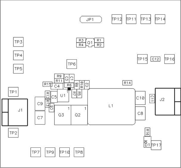 Figure 7-1 TPS40193EVM-001 Component Placement
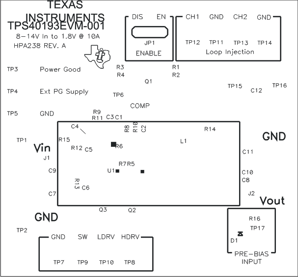 Figure 7-2 TPS40193EVM-001 Silkscreen
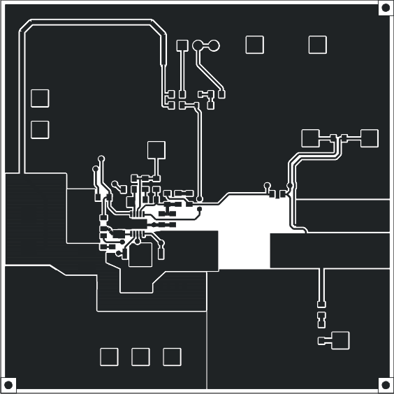 Figure 7-3 TPS40193EVM-001 Top Copper Layer
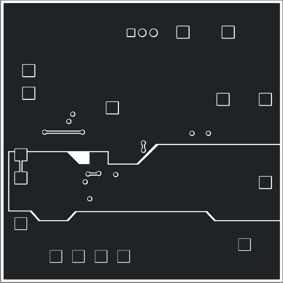 Figure 7-4 TPS40193EVM-001 Bottom Copper Layer
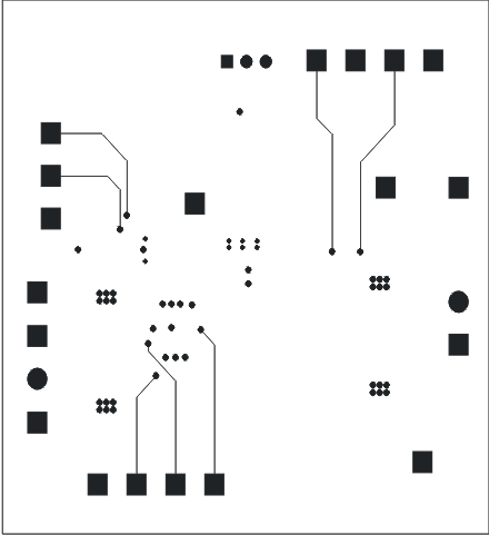 Figure 7-5 TPS40193EVM-001 Internal Layer 1
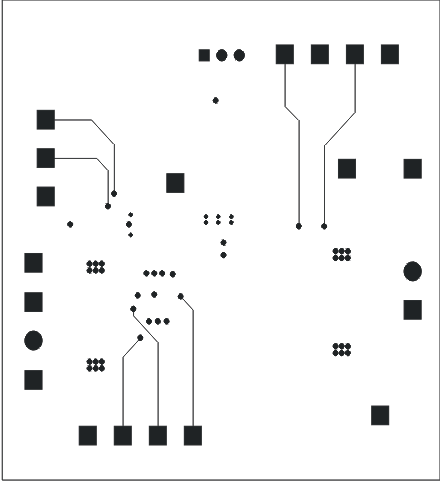 Figure 7-6 TPS40193EVM-001 Internal Layer 2