SLVA514C July 2014 – November 2022 TPS62125
4.2 Input Capacitor Selection
An input capacitor, CIN, is required to provide a local bypass for the input voltage source. A low ESR, X5R or X7R ceramic capacitor is best for input voltage filtering and minimizing interference with other circuits. For most applications, a 10-µF ceramic capacitor is recommended from VIN to ground (system ground, not –VOUT). The CIN capacitor value can be increased without any limit for better input voltage filtering.
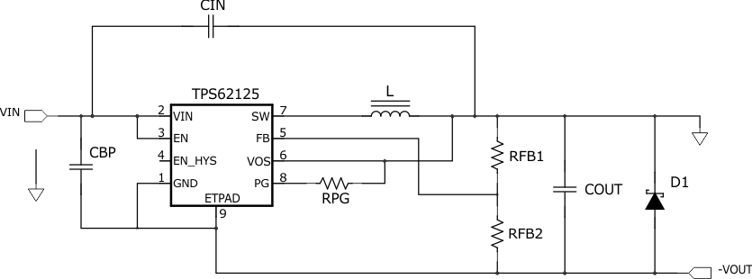
For the inverting buck-boost configuration of the TPS62125, it is not recommended to install a capacitor from VIN to VOUT. Such a capacitor, if installed, provides an AC path from VIN to VOUT. When VIN is applied to the circuit, this dV/dt across a capacitor from VIN to VOUT creates a current that must return to ground (the return of the input supply) to complete its loop. This current might flow through the internal low-side MOSFET's body diode and the inductor to return to ground. Flowing through the body diode pulls the SW pin and VOS pin more than 0.3 V below IC ground, violating their absolute maximum rating. Such a condition might damage the TPS62125 and is not recommended. Therefore, a capacitor from VIN to VOUT is not needed or recommended. If such a capacitor (CBP) is present, then a Schottky diode should be installed on the output, per Figure 4-1. Startup testing should be conducted to ensure that the VOS pin is not driven more than 0.3 V below IC ground when VIN is applied.
 Figure 4-1 If Installing CBP, Installing Schottky D1 is Required
The AC path through CBP might also worsen the line transient response. If strong line transients are expected, the output capacitance should be increased to keep the output voltage within acceptable levels during the line transient.