SLVS757E March 2007 – July 2022 TPS5450
PRODUCTION DATA
- 1 Features
- 2 Applications
- 3 Description
- 4 Revision History
- 5 Pin Configuration and Functions
- 6 Specifications
-
7 Detailed Description
- 7.1 Overview
- 7.2 Functional Block Diagram
- 7.3
Feature Description
- 7.3.1 Oscillator Frequency
- 7.3.2 Voltage Reference
- 7.3.3 Enable (ENA) and Internal Slow-Start
- 7.3.4 Undervoltage Lockout (UVLO)
- 7.3.5 Boost Capacitor (BOOT)
- 7.3.6 Output Feedback (VSENSE) and Internal Compensation
- 7.3.7 Voltage Feed-Forward
- 7.3.8 Pulse-Width-Modulation (PWM) Control
- 7.3.9 Overcurrent Limiting
- 7.3.10 Overvoltage Protection
- 7.3.11 Thermal Shutdown
- 7.4 Device Functional Modes
-
8 Application and Implementation
- 8.1 Application Information
- 8.2
Typical Application
- 8.2.1 Design Requirements
- 8.2.2 Detailed Design Procedure
- 8.2.3 Application Curves
- 9 Power Supply Recommendations
- 10Layout
- 11Device and Documentation Support
- 12Mechanical, Packaging, and Orderable Information
6.6 Typical Characteristics
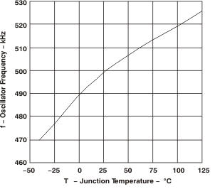 Figure 6-1 Oscillator Frequency vs Junction Temperature
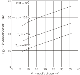 Figure 6-3 Shutdown Quiescent Current vs Input Voltage
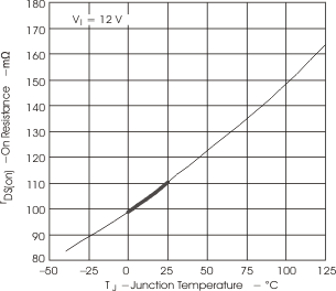 Figure 6-5 On Resistance vs Junction Temperature
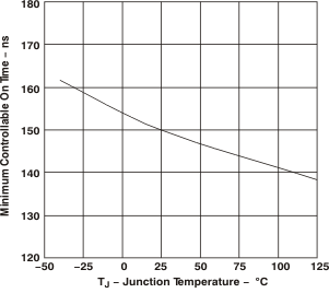 Figure 6-7 Minimum Controllable On Time vs Junction Temperature
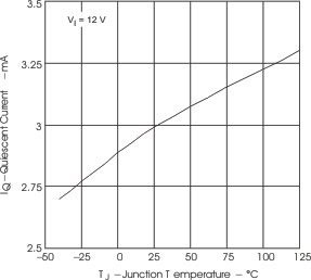 Figure 6-2 Non-Switching Quiescent Current vs Junction Temperature
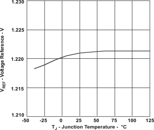 Figure 6-4 Voltage Reference vs Junction Temperature
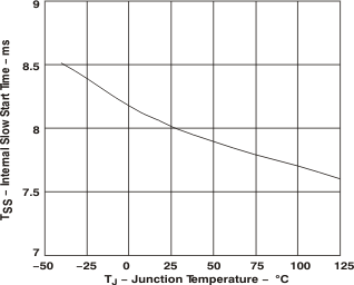 Figure 6-6 Internal Slow Start Time vs Junction Temperature
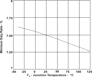 Figure 6-8 Minimum Controllable Duty Ratio vs Junction Temperature