SLVSDK7C April   2017  – February 2020 TPS22971

PRODUCTION DATA.  

  1. Features
  2. Applications
  3. Description
    1.     Device Images
      1.      Typical Application
  4. Revision History
  5. Pin Configuration and Functions
    1.     Pin Functions
  6. Specifications
    1. 6.1 Absolute Maximum Ratings
    2. 6.2 ESD Ratings
    3. 6.3 Recommended Operating Conditions
    4. 6.4 Thermal Information
    5. 6.5 Electrical Characteristics
    6. 6.6 Switching Characteristics
    7. 6.7 Typical DC Characteristics
    8. 6.8 Typical AC Characteristics
  7. Parameter Measurement Information
  8. Detailed Description
    1. 8.1 Overview
    2. 8.2 Functional Block Diagram
    3. 8.3 Feature Description
      1. 8.3.1 On and Off Control
      2. 8.3.2 Controlled Turn-On
      3. 8.3.3 Power Good (PG)
      4. 8.3.4 Quick Output Discharge (QOD)
    4. 8.4 Device Functional Modes
  9. Application and Implementation
    1. 9.1 Application Information
      1. 9.1.1 Thermal Consideration
      2. 9.1.2 PG Pull Up Resistor
      3. 9.1.3 Power Sequencing
    2. 9.2 Typical Application
      1. 9.2.1 Design Requirements
      2. 9.2.2 Detailed Design Procedure
        1. 9.2.2.1 Maximum Voltage Drop and On-Resistance
        2. 9.2.2.2 Managing Inrush Current
      3. 9.2.3 Application Curves
  10. 10Power Supply Recommendations
  11. 11Layout
    1. 11.1 Layout Guidelines
    2. 11.2 Layout Example
  12. 12Device and Documentation Support
    1. 12.1 Documentation Support
      1. 12.1.1 Related Documentation
    2. 12.2 Receiving Notification of Documentation Updates
    3. 12.3 Community Resources
    4. 12.4 Trademarks
    5. 12.5 Electrostatic Discharge Caution
    6. 12.6 Glossary
  13. 13Mechanical, Packaging, and Orderable Information

Typical AC Characteristics

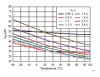
TPS22971 D007_SLVSDK7.gifFigure 5. Turn-On Time vs Temperature
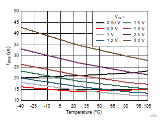
TPS22971 D009_SLVSDK7.gifFigure 7. Rise Time vs Temperature
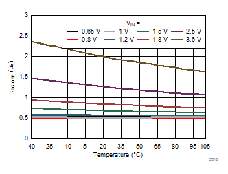
TPS22971 D013_SLVSDK7.gifFigure 9. PG Turn-Off Time vs Temperature
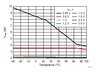
TPS22971 D010_SLVSDK7.gif
RL = 10 Ω CL = 0.1 μF
Figure 11. Fall Time vs Temperature
TPS22971 1p8_Rise.png
RL = 10 Ω CT = 0 pF
TA = 25°C CL = 0.1 µF
Figure 13. Turn-On Response at 1.8 VIN
TPS22971 3p6_Fall.png
RL = 10 Ω CT = 0 pF
TA = 25°C CL = 0.1 µF
Figure 15. Turn-Off Response at 3.6 VIN
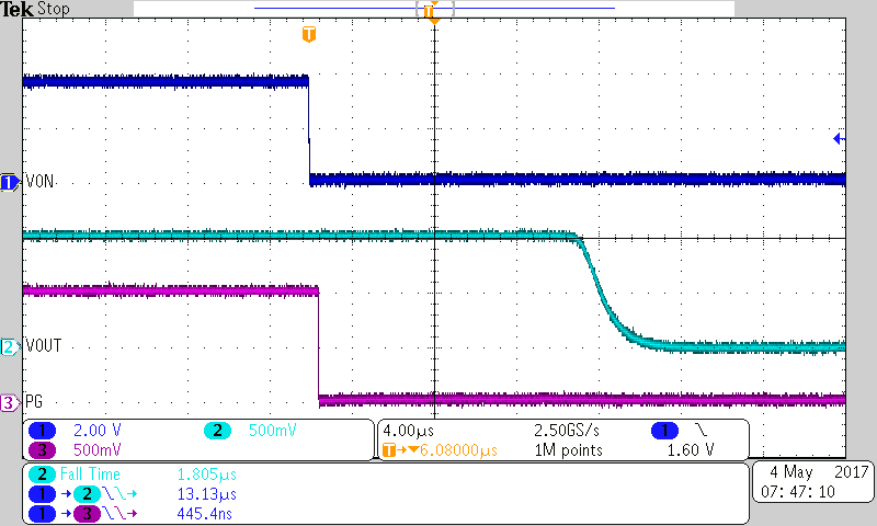
TPS22971 0p65_Fall.png
RL = 10 Ω CIN = 0 pF
TA = 25°C CL = 0.1 µF
Figure 17. Turn-Off Response at 0.65 VIN
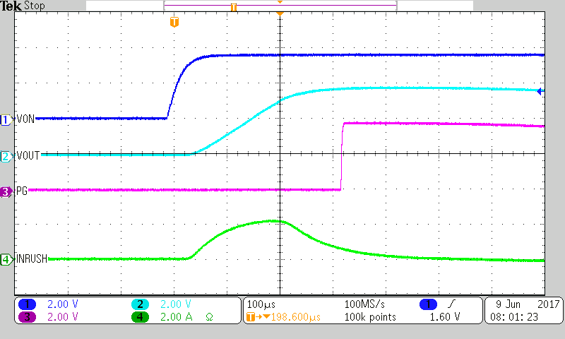
TPS22971 3p6_cout133_ct1000.png
CT = 1000 pF CL = 133 µF
RL = OPEN TA = 25°C
Figure 19. High Inrush Current at 3.6 VIN
TPS22971 0p65_cout133_ct1000.png
CT = 1000 pF CL = 133 µF
RL = OPEN TA = 25°C
Figure 21. High Inrush Current at 0.65 VIN
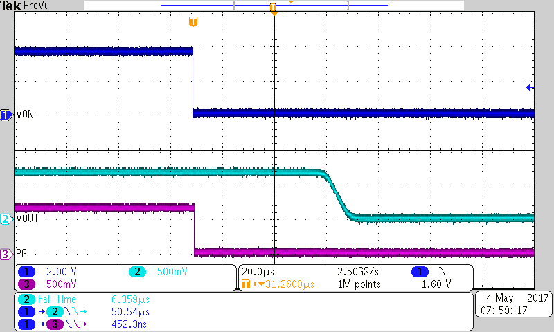
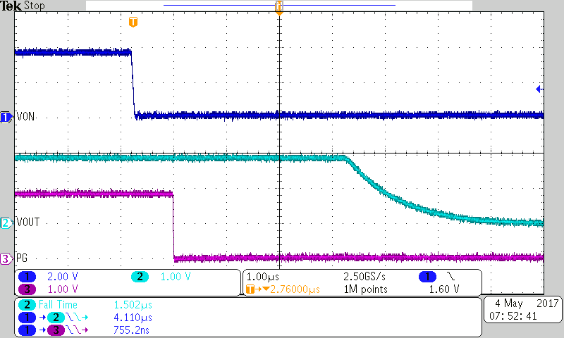
TPS22971 1p0_Fall_Cin10.png
CIN = 0 pF CL = 0.1 µF
RL = 10 Ω TA = 25°C
Figure 23. Fast Turn-Off Response
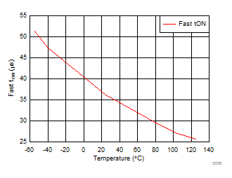
TPS22971 D006_SLVSDK7.gif
VIN = 1V CT = 0 pF CL = 0.1 µF RL = 10 Ω
Figure 6. Fast Turn-On Time vs Temperature
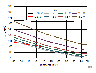
TPS22971 D012_SLVSDK7.gifFigure 8. PG Turn-On Time vs Temperature
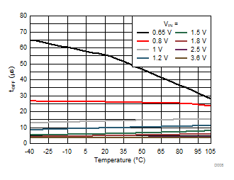
TPS22971 D008_SLVSDK7.gifFigure 10. Turn-Off Time vs Temperature
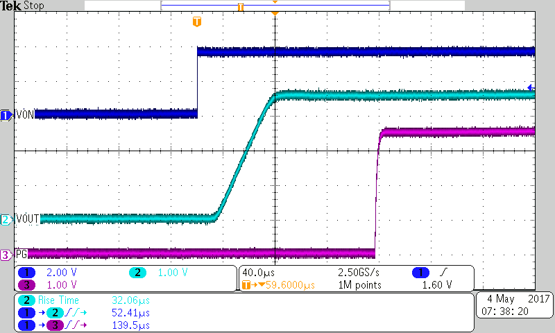
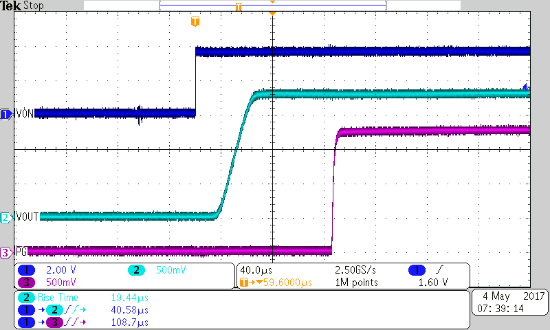
TPS22971 3p6_Rise.png
RL = 10 Ω CT = 0 pF
TA = 25°C CL = 0.1 µF
Figure 12. Turn-On Response at 3.6 VIN
TPS22971 0p65_Rise.png
RL = 10 Ω CT = 0 pF
TA = 25°C CL = 0.1 µF
Figure 14. Turn-On Response at 0.65 VIN
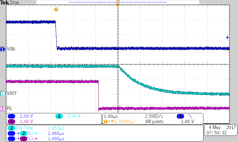
TPS22971 1p8_Fall.png
RL = 10 Ω CT = 0 pF
TA = 25°C CL = 0.1 µF
Figure 16. Turn-Off Response at 1.8 VIN
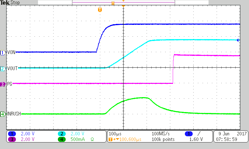
TPS22971 3p6_cout33_ct1000.png
CT = 1000 pF CL = 33 µF
RL = OPEN TA = 25°C
Figure 18. Low Inrush Current at 3.6 VIN
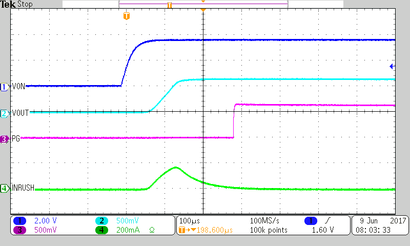
TPS22971 0p65_cout33_ct1000.png
CT = 1000 pF CL = 33 µF
RL = OPEN TA = 25°C
Figure 20. Low Inrush Current at 0.65 VIN
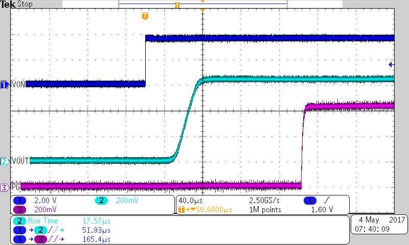
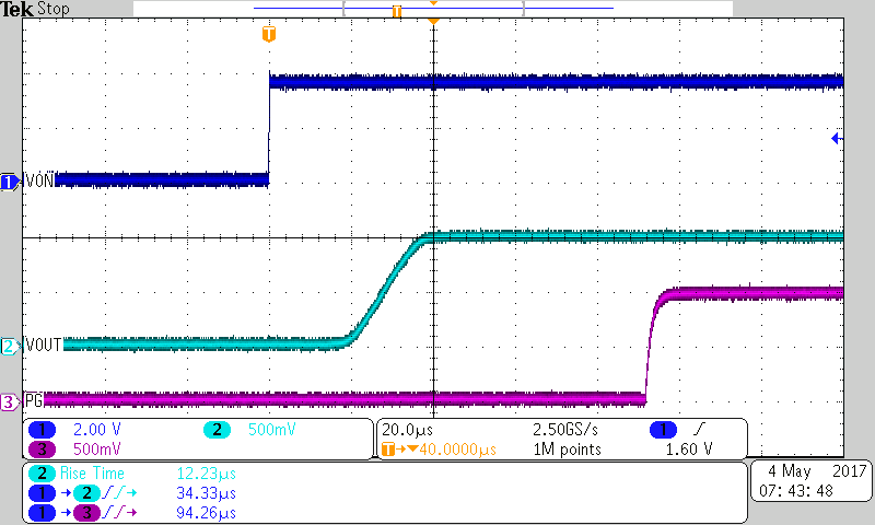
TPS22971 1p0_Rise_Cin10.png
CT = 0 pF CL = 0.1 µF
RL = 10 Ω TA = 25°C
Figure 22. Fast Turn-On Response