SLVU247A July 2008 – October 2021 TPS54331 , TPS54331-Q1
2.9 Powering Up
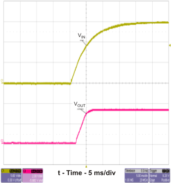
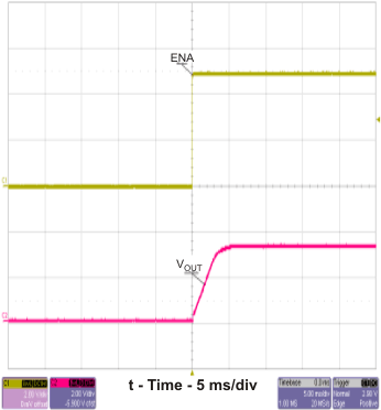
Figure 2-9 and Figure 2-10 shows the start-up waveform. In Figure 2-9, the top trace shows VIN, and the bottom trace shows VOUT. InFigure 2-9, the top trace shows EN (enable) whereas the bottom trace shows VOUT. Initially, the input voltage is applied and the output is inhibited by using a jumper at J2 to tie EN to GND. When the jumper is removed, EN is released. When the EN voltage reaches the enable-threshold voltage of 1.25 V, the start-up sequence begins and the internal reference voltage begins to ramp up at the internally set rate toward 0.8 V and the output voltage ramps up to the externally set value of 3.3 V.
 Figure 2-9 TPS54331 Start-Up
Relative to VIN
 Figure 2-10 TPS5331 Start-Up Relative
to Enable