SLVU952B September 2013 – May 2021 TPS65580
4.8 Start-Up
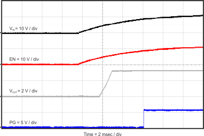
The TPS65580EVM-575 start-up waveform for CH1 relative to VIN is shown in Figure 4-11. Load = 4 Ω resistive. The start up waveforms for CH2 and CH3 are similar and not shown.
 Figure 4-11 TPS65580EVM-575 CH1 Start-Up Relative to VIN
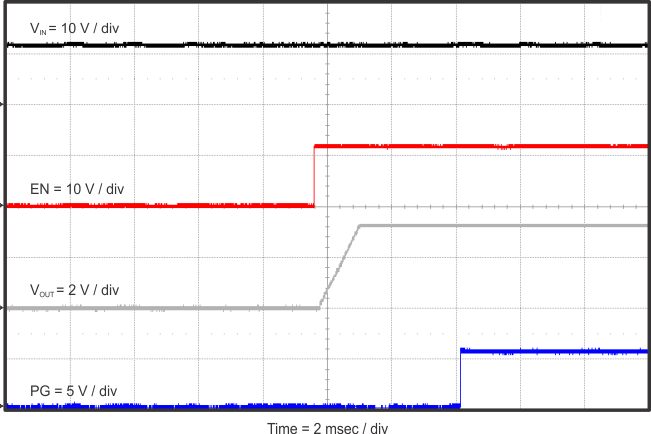
The TPS65580EVM-575 start-up waveform for CH1 relative to enable (EN) is shown in Figure 4-12. Load = 4 Ω resistive. The start up waveforms for CH2 and CH3 are similar and not shown.
 Figure 4-12 TPS65580EVM-575 CH1 Start-Up Relative to EN