SLVUB62B June 2017 – November 2020
- Trademarks
- 1 About this Manual
- 2 Information About Cautions and Warnings
- 3 Items Required for Operation
- 4 Introduction
-
5 Setup
- 5.1
Switch, Push Button, Connector, and Test Point Descriptions
- 5.1.1 Power Path Jumper Configuration
- 5.1.2 DP Source Receptacle
- 5.1.3 S1 HRESET Push-Button
- 5.1.4 S6 SPI MISO Pull Down Button
- 5.1.5 S3: FTDI Enable and Disable
- 5.1.6 S2: SPI , I2C, and BusPowerZ Configurations
- 5.1.7 J1: Barrel Jack Power Connector
- 5.1.8 Barrel Jack Detect
- 5.1.9 USB Type B Connector (J11)
- 5.1.10 USB Type-CConnector (J2)
- 5.1.11 USB Micro B Connector (J9)
- 5.1.12 TP13 (5 V), TP8 (3.3 V), and TP12 (1.2 V)
- 5.1.13 Aardvark Connector (J10)
- 5.1.14 TP10, TP11, TP15, TP16, TP17, TP18, TP9: GND Test Points
- 5.1.15 TP1, TP2, TP3 and TP4 – CC1 and CC2 Test Points
- 5.1.16 TP14 (PA and PB): VBUS Test Point
- 5.1.17 TP7, TP6, and TP5: A-VAR, B-VAR, and System Power Test Points Respectively
- 5.1.18 J3 and J4 (Bottom of EVM): Signal Headers
- 5.2 LED Indicators Description
- 5.1
Switch, Push Button, Connector, and Test Point Descriptions
- 6 Using the TPS65988EVM
- 7 Connecting the EVM
- 8 REACH Compliance
- 9 TPS65988EVM Schematic
- 10TPS65988EVM Board Layout
- 11TPS65988EVM Bill of Materials
- 12Revision History
5.1.6 S2: SPI , I2C, and BusPowerZ Configurations
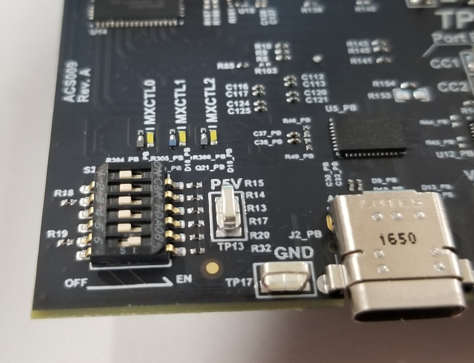
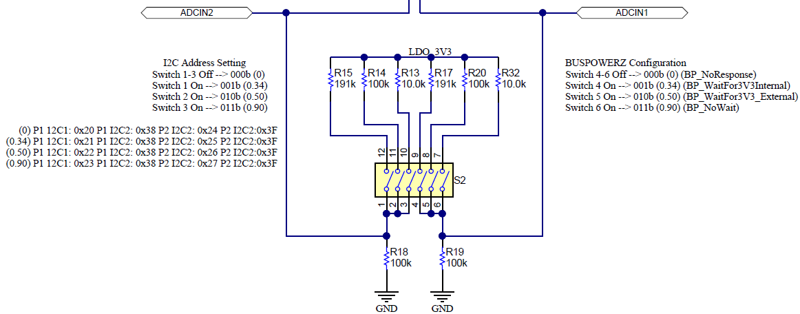
The TPS65988EVM has a dip switch (S2) that can be used to configure the I2C addresses and BusPower settings of the device. Switch1 through Switch3 are used to set the I2C address of the TPS65988 by adjusting the voltage divider seen at ADCIN2. Refer to the TPS65988 datasheet to see the different I2C address configurations. The default switch setting for Switch 1 through switch 3 is open, resulting in a 0x38 I2C address. Switch4 through Switch6 adjusts the BusPowerZ setting by adjusting the voltage divider on ADCIN1. Refer to the TPS65988 datasheet to see the different BusPowerZ configurations. Figure 5-15 highlights the default switch setting of S2.
 Figure 5-15 I2C and BusPower DIP Switch (S2)
 Figure 5-16 I2C DIP Switch (S2) Schematic