SLYT821 January 2022 AFE0064 , AFE1256 , AFE2256 , AFE3256 , DDC112 , DDC1128 , DDC114 , DDC118 , DDC232 , DDC264 , DDC316
2 DDC
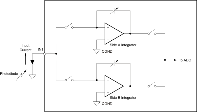
The DDC family extends from a two-channel device (the DDC112) all the way to a 256-channel device (the DDC2256), with intermediate versions for four, eight, 16, 32, 64 and 128 channels. Every DDC channel outputs a digital value corresponding to the integration (charge) of an input current between two instants (two consecutive edges of a clock signal). Engineers can see the DDCs as a transimpedance amplifier followed by an ADC equivalently, where instead of a resistor, a combination of the feedback capacitor and integration time (sampling rate) sets the gain (see Figure 2-1).
 Figure 2-1 A dual-integrator DDC input
architecture
Figure 2-1 A dual-integrator DDC input
architectureIn applications such as computed tomography scanners or fluorescence measurements, getting a charge value as the numerical device output has the advantage of directly providing, with a single reading, a value proportional to the total number of photons incident on the photodiode during that interval (instead of sampling the signal continuously and adding up the samples later). The signal does not have to be continuous during that time and the DDC’s input integrator integrates even fast current pulses between two edges. The bandwidth of the front-end integrator is actually larger (approximately in the megahertz range) than what the sample rate could lead one to believe.
For applications in which users prefer to process the data in current units, dividing the charge result by the integration period (the time between the two edges) obtains the average current value. Any temporal information in that interval will be lost and translated into a single average current sample.
Depending on the DDC device, it is possible to adjust the sampling rate (the inverse of the integration period) from 1 SPS to 100 kSPS (with the DDC316 only at 12 bits). A more standard value for the maximum sample rate for most DDCs is around 6 kSPS per channel with 20-bit resolution. Table 2-1 summarizes the top-level specifications for each device in the DDC family.
| Device Name | Number of Channels | Minimum Maximum Channel Sample Rate [kSPS] | Maximum Full-Scale Charge [pC] | Maximum Full-Scale Current [µA] | Power [mW/ Channel] | Number of Bits |
|---|---|---|---|---|---|---|
| DDC112 | 2 | 0.001-3 | 1,000 | 3 | 85 | 20 |
| DDC114 | 4 | 0.001-3 | 350 | 1 | 18 | 20 |
| DDC118 | 8 | 0.001-3 | 350 | 1 | 18 | 20 |
| DDC316 | 16 | 1-100 | 12 | 1.2 | 28 | 12 at 100 kSPS 16 at 50 kSPS |
| DDC232 | 32 | 0.001-6 | 350 | 2 | 10 | 20 |
| DDC264 | 64 | 0.001-6 | 150 | 1 | 5.5 | 20 |
| DDC1128 | 128 | 0.001-6 | 150 | 1 | 5.5 | 20 |
| DDC2256 | 256 | 1-17 | 150 | 2.5 | 2 | 24 |
The devices’ programmable full scale (swapping the integration capacitor) enables you to optimize the noise floor for a given application, assay or run, which is particularly important for instrumentation applications. Increasing the input gain will lower the noise floor down to 0.2 fCrms (1,250 electrons). Nevertheless, larger dynamic ranges are obtained at the lower gains (higher full-scale inputs), with typical values around 90 dB.
With current computed as the charge divided by the integration time, the maximum current (in the linear range) is given by the maximum full-scale charge setting and minimum integration time. Table 2-1 also lists these results. Typical maximum full-scale charges range from 150 pC to 350 pC, although the DDC112 enables the use of an external feedback capacitor that can take the range beyond 1 nC. In current units, the maximum range will be approximately 1 µA.
One major difference between the X-ray AFE and DDC families is that DDCs can only measure current flowing into the input terminal. That said, all DDCs have about 0.4% of the full scale as margin for currents leaving the terminal, which enables calibration of the offset at the zero-current point. Also, there are relatively simple techniques that enable the measurement of negative currents with an external resistor [3].
Finally, the devices come in leaded or ball-grid array (BGA) packages, which makes their handling straightforward through standard assembly methods.