SLYY221 November 2023 ADC12DJ5200RF , ADS124S08 , ADS127L11 , AFE2256 , REF35 , REF70 , TPS62912 , TPS62913 , TPS7A94 , TPSM82912 , TPSM82913 , UCC5880-Q1
- 1
- Overview
- At a glance
- Why high voltage?
- Optimizing wide-bandgap FET performance with component innovations
- Selecting the right gate drivers
- Selecting the right controllers
- Maximizing power density with topology innovations
- Achieving extreme efficiency targets with system-level innovation
- Addressing EMI challenges
- Conclusion
- Additional resources
Optimizing wide-bandgap FET performance with component innovations
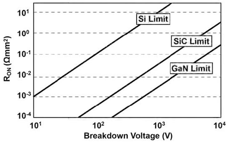
Wide-bandgap FETs such as silicon carbide (SiC) MOSFETs or gallium nitride (GaN) FETs offer a higher-efficiency alternative to silicon MOSFETs. Wide band-gap FETs have very low or even not reverse recovered charge (Qrr), as well as lower on-resistance under the same voltage levels as silicon MOSFETs, shown in Figure 1.
 Figure 1 Theoretical on-resistance vs.
blocking voltage.
Figure 1 Theoretical on-resistance vs.
blocking voltage.In addition, almost all other parasitics including gate charge (Qg) and output capacitance (Coss) are much lower in wide band-gap FETs than silicon MOSFETs, leading to much faster switching speeds: an over 150-V/ns slew rate compared to a superjunction silicon MOSFET’s less than 80-V/ns slew rate. With faster switching speeds, the time it takes for power switches to turn on or off is shorter, and switching losses are reduced.