SNAS722B december 2017 – august 2023 LMK61E07
PRODUCTION DATA
- 1
- 1 Features
- 2 Applications
- 3 Description
- 4 Revision History
- 5 Pin Configuration and Functions
-
6 Specifications
- 6.1 Absolute Maximum Ratings
- 6.2 ESD Ratings
- 6.3 Recommended Operating Conditions
- 6.4 Thermal Information
- 6.5 Electrical Characteristics - Power Supply
- 6.6 LVPECL Output Characteristics
- 6.7 LVDS Output Characteristics
- 6.8 HCSL Output Characteristics
- 6.9 Frequency Tolerance Characteristics
- 6.10 Frequency Margining Characteristics
- 6.11 Power-On Reset Characteristics (VDD)
- 6.12 I2C-Compatible Interface Characteristics (SDA, SCL)
- 6.13 PSRR Characteristics
- 6.14 Other Characteristics
- 6.15 PLL Clock Output Jitter Characteristics
- 6.16 Typical 156.25-MHz Output Phase Noise Characteristics
- 6.17 Typical 161.1328125 MHz Output Phase Noise Characteristics
- 6.18 Additional Reliability and Qualification
- 6.19 Typical Characteristics
- 7 Parameter Measurement Information
-
8 Detailed Description
- 8.1 Overview
- 8.2 Functional Block Diagram
- 8.3
Feature Description
- 8.3.1 Device Block-Level Description
- 8.3.2 Device Configuration Control
- 8.3.3 Register File Reference Convention
- 8.3.4 Configuring the PLL
- 8.3.5 Integrated Oscillator
- 8.3.6 Reference Divider and Doubler
- 8.3.7 Phase Frequency Detector
- 8.3.8 Feedback Divider (N)
- 8.3.9 Fractional Engine
- 8.3.10 Charge Pump
- 8.3.11 Loop Filter
- 8.3.12 VCO Calibration
- 8.3.13 High-Speed Output Divider
- 8.3.14 High-Speed Clock Output
- 8.3.15 Device Status
- 8.4 Device Functional Modes
- 8.5 Programming
- 8.6
Register Maps
- 8.6.1
Register Descriptions
- 8.6.1.1 VNDRID_BY1 Register; R0
- 8.6.1.2 VNDRID_BY0 Register; R1
- 8.6.1.3 PRODID Register; R2
- 8.6.1.4 REVID Register; R3
- 8.6.1.5 TARGETADR Register; R8
- 8.6.1.6 EEREV Register; R9
- 8.6.1.7 DEV_CTL Register; R10
- 8.6.1.8 XO_CAPCTRL_BY1 Register; R16
- 8.6.1.9 XO_CAPCTRL_BY0 Register; R17
- 8.6.1.10 DIFFCTL Register; R21
- 8.6.1.11 OUTDIV_BY1 Register; R22
- 8.6.1.12 OUTDIV_BY0 Register; R23
- 8.6.1.13 RDIVCMOSCTL Register; R24
- 8.6.1.14 PLL_NDIV_BY1 Register; R25
- 8.6.1.15 PLL_NDIV_BY0 Register; R26
- 8.6.1.16 PLL_FRACNUM_BY2 Register; R27
- 8.6.1.17 PLL_FRACNUM_BY1 Register; R28
- 8.6.1.18 PLL_FRACNUM_BY0 Register; R29
- 8.6.1.19 PLL_FRACDEN_BY2 Register; R30
- 8.6.1.20 PLL_FRACDEN_BY1 Register; R31
- 8.6.1.21 PLL_FRACDEN_BY0 Register; R32
- 8.6.1.22 PLL_MASHCTRL Register; R33
- 8.6.1.23 PLL_CTRL0 Register; R34
- 8.6.1.24 PLL_CTRL1 Register; R35
- 8.6.1.25 PLL_LF_R2 Register; R36
- 8.6.1.26 PLL_LF_C1 Register; R37
- 8.6.1.27 PLL_LF_R3 Register; R38
- 8.6.1.28 PLL_LF_C3 Register; R39
- 8.6.1.29 PLL_CALCTRL Register; R42
- 8.6.1.30 NVMSCRC Register; R47
- 8.6.1.31 NVMCNT Register; R48
- 8.6.1.32 NVMCTL Register; R49
- 8.6.1.33 NVMLCRC Register; R50
- 8.6.1.34 MEMADR Register; R51
- 8.6.1.35 NVMDAT Register; R52
- 8.6.1.36 RAMDAT Register; R53
- 8.6.1.37 NVMUNLK Register; R56
- 8.6.1.38 INT_LIVE Register; R66
- 8.6.1.39 SWRST Register; R72
- 8.6.1
Register Descriptions
- 9 Application and Implementation
- 10Device and Documentation Support
- 11Mechanical, Packaging, and Orderable Information
3 Description
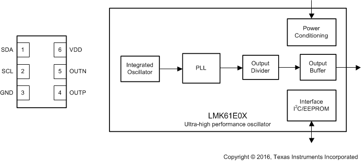
The LMK61E07 family of ultra-low jitter PLLatinum™ programmable oscillators uses fractional-N frequency synthesizers with integrated VCOs to generate commonly used reference clocks. The output on LMK61E07 can be configured as LVPECL, LVDS, or HCSL. The device features self-start-up from on-chip EEPROM to generate a factory-programmed default output frequency, or the device registers and EEPROM settings are fully programmable in-system through an I2C serial interface. The device provides fine and coarse frequency margining control through an I2C serial interface, making it a digitally-controlled oscillator (DCXO).
The PLL feedback divider can be updated to adjust the output frequency without spikes or glitches in steps of <1ppb using a PFD of 12.5 MHz (R divider=4, doubler disabled) for compatibility with xDSL requirements, or in steps of <5.2 ppb using a PFD of 100 MHz (R divider=1, doubler enabled) for compatibility with broadcast video requirements. The frequency margining features also facilitate system design verification tests (DVT), such as standards compliance and system timing margin testing.
 Pinout and Simplified Block Diagram