SNAU287 November 2023
- 1
- Description
- Features
- 4
- 1Evaluation Module Overview
- 2Hardware
- 3Software
- 4Hardware Design Files
- 5Additional Information
- 6Related Documentation
3.1.1.2 Output Formats
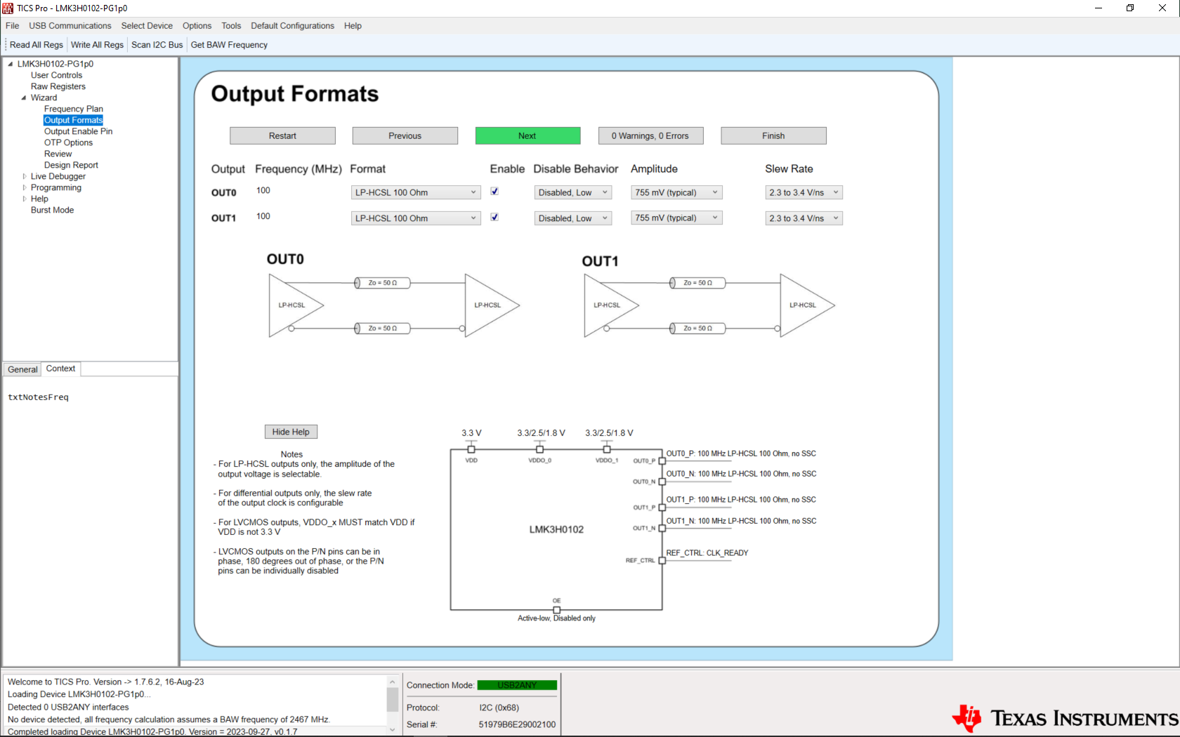
 Figure 3-3 LMK3H0102 Wizard Output Formats Page
The Output Formats page allows for configuring the formats of the device outputs. For each output type selected, the images in the GUI change to provide a visual aid. For differential outputs, these are diagrams showing the termination required. For single-ended outputs, these are diagrams showing the behavior of the P and N pins of the output.
If an LP-HCSL output is selected, Amplitude field sets the typical LP-HCSL amplitude. If an LVDS output is selected, then this field is hidden as the settings do not apply to LVDS. For LVCMOS outputs, the phase is selectable, and the field changes to a Phase field. The OUTx_P and OUTx_N pins can be individually enabled, in phase, or opposite phase.
For all differential outputs, the output slew rate can be configured using the Slew Rate field. For single-ended outputs, the phase and LVCMOS voltages are selectable, and the Slew Rate field changes to an LVCMOS Voltage field. The LVCMOS Voltage is not register-backed, but instead is meant to provide a visual by displaying the pin voltage in the block diagram.
Each output can be individually enabled or disabled on this page. A disabled output can be pulled to GND internally or tr-istated. By default, any disabled outputs are pulled to GND.