SNLU210C July   2016  – April 2024 DS90UB933-Q1


  1.   1
  2.   Description
  3.   Features
  4.   4
  5. 1Evaluation Module Overview
    1. 1.1 Introduction
    2. 1.2 Kit Contents
  6. 2Hardware
    1. 2.1 Requirements
    2. 2.2 Major Components of DS90UB933-Q1EVM
    3. 2.3 Board Setup Details
      1. 2.3.1 Power Connections
      2. 2.3.2 FPD-Link III Connection
      3. 2.3.3 LVCMOS Input Connector Description (on DS90UB933-Q1 Board)
      4. 2.3.4 Factory Set Switch Settings and Jumpers Default Configuration
        1. 2.3.4.1 Serializer Board Default Configuration
    4. 2.4 Operation with Deserializer
    5. 2.5 Troubleshooting the EVM Setup
  7. 3Software
    1. 3.1 Using I2C
      1. 3.1.1 Default Addresses
      2. 3.1.2 Analog Launch Pad (ALP)
  8. 4Hardware Design Files
    1. 4.1 Schematics
    2. 4.2 PCB Layout
      1. 4.2.1 DS90UB933-Q1EVM Serializer Board Layout
    3. 4.3 DS90UB933-Q1EVM Serializer Board Bill of Materials
  9. 5Additional Information
    1. 5.1 Trademarks
  10. 6Revision History

FPD-Link III Connection

The FPD-Link III serial stream comes out of CN1 on the serializer board as a single-ended signal. Connect to the corresponding connector on the deserializer board. DOUT- on the Serializer and RIN- on the deserializer are terminated to ground through 47nF capacitors in series with 50Ω termination.
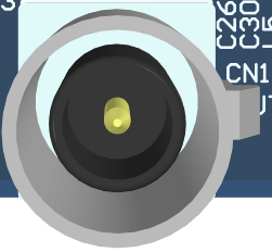
GUID-20240411-SS0I-Z751-FK5D-4B4TWL7CRN8K-low.pngFigure 2-2 Serial Link Connection Using a Single 50Ω Coaxial Cable