SNOA997A July 2018 – August 2019 TLV7031
Design Goals
| Output | Thresholds | Supply | |||||
|---|---|---|---|---|---|---|---|
| V0 = HIGH | Vo = LOW | VH | VL | VHYS | Vcc | VPU | Vref |
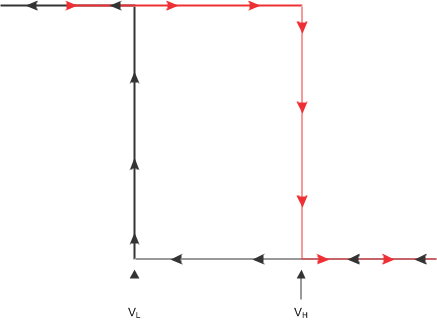
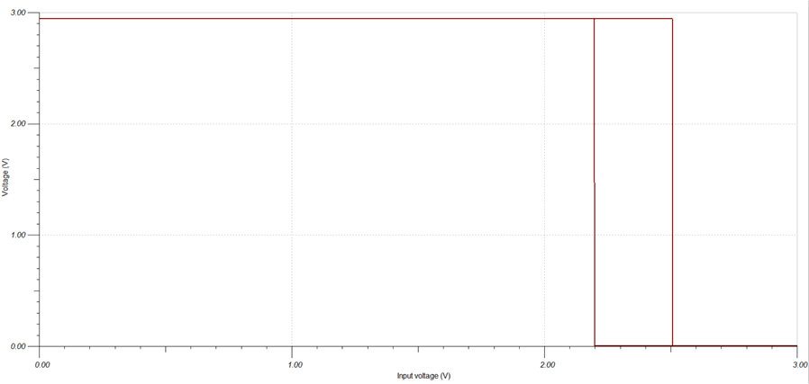
| Vi < VL | Vi > VH | 2.5 V | 2.2 V | 300 mV | 3 V | 3 V | 3 V |
Design Description
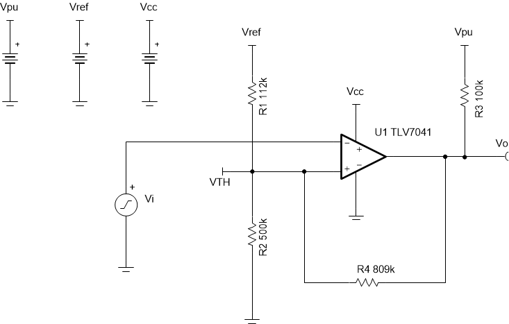
Comparators are used to differentiate between two different signal levels. With noise, signal variation, or slow-moving signals, undesirable transitions at the output can be observed with a constant threshold. Setting upper and lower hysteresis thresholds eliminates these undesirable output transitions. This circuit example will focus on the steps required to design the positive feedback resistor network necessary to obtain the desired hysteresis for an inverting comparator application.
Design Notes
- The accuracy of the hysteresis threshold voltages are related to the tolerance of the resistors used in the circuit, the selected comparator’s input offset voltage specification, and any internal hysteresis of the device.
- The TLV7041 has an open-drain output stage, so a pull-up resistor is needed.
Design Steps
- Select the lower biasing resistor,
R2. This resistor can be modified for any design. In this case,
it is assumed that power conservation is necessary, therefore, R2 is
selected to be large.
- Select the switching thresholds for when the comparator will
transition from high to low (VL) and low to high (VH).
VL is the necessary input voltage for the comparator output to
transition low and VH is the required input voltage for the
comparator to output high.
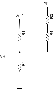
- Analyze the circuit when the input voltage is VH. At this
point, Vo=3 V=VPU and the transition to a logic low is
initiated in the comparator output. Using Kirchhoff's Current Law, solve for an
equation for R1.
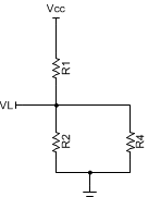
- Analyze the circuit when the input
voltage is VL. At this point, Vo=0 V and the transition to
a logic high is initiated in the comparator output. Using Kirchhoff's Current
Law, solve for an equation for R1.
- After defining some constants, set
the two equations for R1 equal to obtain a quadratic equation for
R4.
-
- If the output stage is
push-pull, then make the following modifications to the above equations:
-
- Solve the quadratic equation for
R4 and pick the most logical result.
- Calculate R1 by
substituting the value for the A constant into the equation for
R1 found in step 4.
DC Transfer Simulation Results
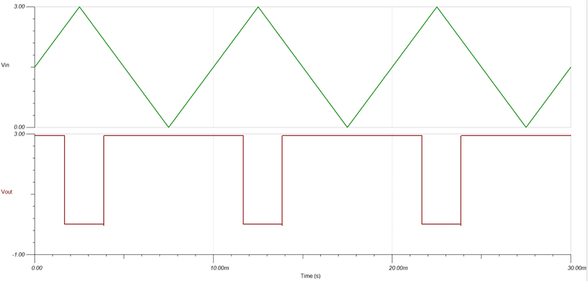
Transient Simulation Results
Design References
See Analog Engineer's Circuit Cookbooks for TI's comprehensive circuit library.
See Comparator with Hysteresis Reference Design TIPD144.
See Circuit SPICE Simulation File SLVMCQ0, Inverting Comparator with Hysteresis Circuit Reference Design.
For more information on many comparator topics including hysteresis, propagation delay and input common mode range please see TI Precision Labs – Op amps.
Design Featured Comparator
| TLV7031 / TLV7041 | |
|---|---|
| Output Type | PP (7031) / OD (7041) |
| Vcc | 1.6V to 6.5V |
| VinCM | Rail-to-rail |
| Vos | ±100 µV |
| VHYS | 7 mV |
| Iq | 335 nA/Ch |
| tpd | 3 µs |
| #Channels | 1 and 2 |
| TLV7041 | |
Design Alternate Comparator