SNVAA73 may 2023 LM53602 , LM53602-Q1 , LM53603-Q1 , LM63625-Q1 , LM63635-Q1 , LMR14020-Q1 , LMR14030-Q1
4 Using a Boot Resistor
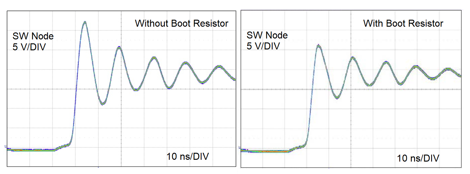
The charge-pump circuit in Figure 1-1 uses CBOOT to boost the high-side gate supply above the supply voltage of the power stage. One method to reduce ringing is to include a boot resistor in series with the boot capacitor, which slows down the turn on speed of the high side NFET as shown in Figure 5-2. This method allows more time for the parasitic network to discharge, ultimately limiting the ringing shown in Figure 4-1. The value of the boot resistor is determined by starting at 0 and increasing the resistance until the desired ringing or EMI level is achieved.
 Figure 4-1 Reduce SW Ringing by RBOOT