SNVSA75D November 2015 – May 2017 LP8862-Q1
PRODUCTION DATA.
- 1 Features
- 2 Applications
- 3 Description
- 4 Revision History
- 5 Device Comparison Table
- 6 Pin Configuration and Functions
-
7 Specifications
- 7.1 Absolute Maximum Ratings
- 7.2 ESD Ratings
- 7.3 Recommended Operating Conditions
- 7.4 Thermal Information
- 7.5 Electrical Characteristics
- 7.6 Internal LDO Electrical Characteristics
- 7.7 Protection Electrical Characteristics
- 7.8 Power Line FET Control Electrical Characteristics
- 7.9 Current Sinks Electrical Characteristics
- 7.10 PWM Brightness Control Electrical Characteristics
- 7.11 Boost or SEPIC Converter Characteristics
- 7.12 Logic Interface Characteristics
- 7.13 Typical Characteristics
- 8 Detailed Description
- 9 Application and Implementation
- 10Power Supply Recommendations
- 11Layout
- 12Device and Documentation Support
- 13Mechanical, Packaging, and Orderable Information
9 Application and Implementation
9.1 Application Information
The LP8862-Q1 is designed for automotive applications, and an input voltage VIN is intended to be connected to the automotive battery. Device circuitry is powered from the internal LDO, which can alternatively be used as an external VDD voltage — in this case external voltage should be in 4.5-V to 5.5-V range.
The LP8862-Q1 uses a simple four-wire control:
- VDDIO/EN for enable
- PWM input for brightness control
- SYNC pin for boost synchronisation (optional)
- FAULT output to indicate fault condition (optional)
9.2 Typical Applications
9.2.1 Typical Application for 2 LED Strings
Figure 19 shows typical application for the LP8862-Q1 which supports 2 LED strings with maximum current 160 mA per string. Boost switching frequency in this example is is 400 kHz.
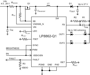 Figure 19. LP8862-Q1 Boost Mode, Two Strings, 160-mA String Configuration
9.2.1.1 Design Requirements
Typical design parameters for a boost-mode two-string configuration are shown in Table 4:
Table 4. Boost Mode Design Parameters
| DESIGN PARAMETER | VALUE |
|---|---|
| VIN voltage range | 4.5…28 V |
| LED string | 2 × 8 LEDs (30 V) |
| LED string current | 160 mA |
| Max boost voltage | 37 V |
| Boost switching frequency | 400 kHz |
| External boost sync | not used |
| Boost spread spectrum | enabled |
| L1 | 22 μH |
| CIN | 10 µF, 50 V |
| CIN BOOST | 2 × (10-µF 50-V ceramic) + 33-µF 50-V electrolytic |
| COUT | 2 × (10-µF 50-V ceramic) + 33-µF 50-V electrolytic |
| CFB | 15 pF |
| CLDO | 1 µF, 10 V |
| RISET | 30 kΩ |
| RFSET | 160 kΩ |
| RISENSE | 50 mΩ |
| R1 | 750 kΩ |
| R2 | 130 kΩ |
| R3 | 10 kΩ |
| RGS | 20 kΩ |
9.2.1.2 Detailed Design Procedure
9.2.1.2.1 Inductor Selection
There are two main considerations when choosing an inductor; the inductor must not saturate, and the inductor current ripple must be small enough to achieve the desired output voltage ripple. Different saturation current rating specifications are followed by different manufacturers so attention must be given to details. Saturation current ratings are typically specified at 25°C. However, ratings at the maximum ambient temperature of application should be requested from the manufacturer. Shielded inductors radiate less noise and are preferred. The saturation current must be greater than the sum of the maximum load current and the worst case average-to-peak inductor current. Equation 4 shows the worst-case conditions:
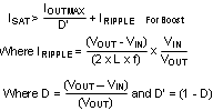
where
- IRIPPLE - peak inductor current
- IOUTMAX - maximum load current
- VIN - minimum input voltage in application
- L - min inductor value including worst case tolerances
- f - minimum switching frequency
- VOUT - output voltage
- D - Duty Cycle for CCM Operation
- VOUT - Output Voltage
As a result the inductor must be selected according to the ISAT. A more conservative and recommended approach is to choose an inductor that has a saturation current rating greater than the maximum current limit. A saturation current rating of at least 3 A is recommended for most applications. See Table 2 for inductance recommendations for the different switching frequency ranges. Resistance of the inductor must be less than 300 mΩ for good efficiency.
See detailed information in Understanding Boost Power Stages in Switch Mode Power Supplies. “Power Stage Designer™ Tools” can be used for the boost calculation: http://www.ti.com/tool/powerstage-designer.
9.2.1.2.2 Output Capacitor Selection
A ceramic capacitor with 2 × VMAX BOOST or more voltage rating is recommended for the output capacitor. The DC-bias effect can reduce the effective capacitance by up to 80%, which needs to be considered in capacitance value selection. Capacitance recommendations for different boost switching frequencies are shown in Table 2. To minimize audible noise of ceramic capacitors their geometric size must typically be minimized.
9.2.1.2.3 Input Capacitor Selection
A ceramic capacitor with 2 × VVIN MAX or more voltage rating is recommended for the input capacitor. The DC-bias effect can reduce the effective capacitance by up to 80%, which needs to be considered in capacitance value selection. Capacitance recommendations for different boost switching frequencies are shown in Table 2.
9.2.1.2.4 LDO Output Capacitor
A ceramic capacitor with at least 10-V voltage rating is recommended for the output capacitor of the LDO. The DC-bias effect can reduce the effective capacitance by up to 80%, which needs to be considered in capacitance value selection. Typically a 1-µF capacitor is sufficient.
9.2.1.2.5 Diode
A Schottky diode should be used for the boost output diode. Do not use ordinary rectifier diodes, since slow switching speeds and long recovery times cause the efficiency and the load regulation to suffer. Diode rating for peak repetitive current must be greater than inductor peak current (up to 3 A) to ensure reliable operation. Average current rating must be greater than the maximum output current. Schottky diodes with a low forward drop and fast switching speeds are ideal for increasing efficiency. Choose a reverse breakdown voltage of the Schottky diode significantly larger than the output voltage.
9.2.1.2.6 Power Line Transistor
A pFET transistor with necessary voltage rating (VDS at least 5 V higher than max input voltage) must be used. Current rating for the FET must be the same as input peak current or greater. Transfer characteristic is very important for pFET. VGS for open transistor must be less than VIN. A 20-kΩ resistor between pFET gate and source is sufficient.
9.2.1.2.7 Input Current Sense Resistor
A high-power 50 mΩ resistor must be used for sensing the boost input current. Power rating can be calculated from the input current and sense resistor resistance value. Increasing RISENSE decreases VIN_OCP current proportionally.
9.2.1.3 Application Curves
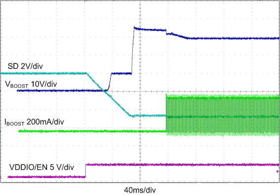
| ƒSW = 300 kHz | VIN = 10 V | |
| Brightness PWM 50% 100 Hz | ||
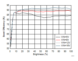
| Two strings, 8 LEDs per string | ƒSW = 400 kHz | |
| 160 mA/string for VIN = 12 V and VIN = 16 V | ||
| 130 mA/string for VIN = 8 V | ||
| 90 mA/string for VIN = 5 V | ||
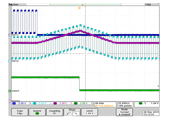
| Open string connected to OUT1 |
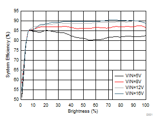
| Two strings, 8 LEDs per string | fSW = 400 kHz | |
| 160 mA/string for VIN = 12 V and VIN = 16 V | ||
| 130 mA/string for VIN = 8 V | ||
| 90 mA/string for VIN = 5 V | ||
9.2.2 SEPIC Mode Application
When LED string voltage can be above or below VIN voltage, SEPIC configuration can be used. In Figure 24 an external frequency is used to synchronize SEPIC switching frequency. External frequency can be modulated to spread switching frequency spectrum.
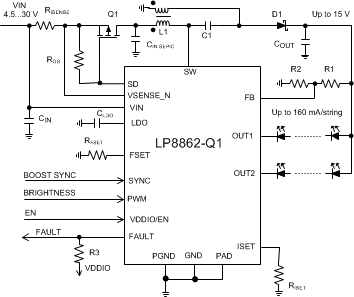 Figure 24. SEPIC Mode, 2 Strings, 160-mA String Configuration
Typical design parameters for a SEPIC-mode two-string configuration are shown in Table 5:
Table 5. SEPIC Mode Design Parameters
| DESIGN PARAMETER | VALUE |
|---|---|
| VIN voltage range | 4.5…30 V |
| LED string | 2 × 2 LEDs (9 V) |
| LED string current | 160 mA |
| Max output voltage | 15 V |
| SEPIC switching frequency | 300 kHz |
| External boost sync | used |
| Spread spectrum | Internal spread spectrum not available, external frequency input can be modulated |
| L1 | 22 μH |
| CIN | 10 µF, 50 V |
| CIN SEPIC | 2 × (10-µF 50-V ceramic) + 33-µF 50-V electrolytic |
| COUT | 2 × (10-µF 50-V ceramic) + 33-µF 50-V electrolytic |
| CLDO | 1 µF, 10 V |
| RISET | 30 kΩ |
| RFSET | 210 kΩ |
| RISENSE | 50 mΩ |
| R1 | 300 kΩ |
| R2 | 130 kΩ |
| R3 | 10 kΩ |
| RGS | 20 kΩ |
9.2.2.1 Detailed Design Procedure
In SEPIC mode the maximum voltage at the SW pin is equal to the sum of the input voltage and the output voltage. Because of this, the maximum sum of input and output voltage must be limited below 50 V. See Detailed Design Procedure for general external component guidelines. The main differences of SEPIC compared to boost are described below.
Power Stage Designer™ Tool can be used for modeling SEPIC behavior: http://www.ti.com/tool/powerstage-designer. For detailed explanation on SEPIC see Texas Instruments Analog Applications Journal Designing DC/DC Converters Based on SEPIC Topology (SLYT309).
9.2.2.1.1 Inductor
In SEPIC mode, coupled coil saturation rating should be higher than input side inductor peak current. Current values can be estimated using Power Stage Designer™ Tool or using equations in SLYT309.
9.2.2.1.2 Diode
In SEPIC mode diode peak current is equal to the sum of input and output currents. Diode rating for peak repetitive current must be greater than SW pin current limit (up to 3 A for transients) to ensure reliable operation. Average current rating must be greater than the maximum output current. Voltage rating must be higher than sum of input and output voltages.
9.2.2.1.3 Capacitor C1
A ceramic capacitor with low ESR is recommended. Voltage rating must be higher than maximum input voltage.
9.2.2.2 Application Curves
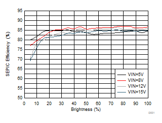
| Two strings, 2 LEDs per string | ƒSW = 300 kHz | |
| 160 mA/string | ||
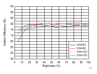
| Two strings, 2 LEDs per string | fSW = 300 kHz | |
| 160 mA/string | ||