SPRADC3 june 2023 AM2431 , AM2432 , AM2434 , AM2631 , AM2631-Q1 , AM2632 , AM2632-Q1 , AM2634 , AM2634-Q1 , AM263P4 , AM3351 , AM3352 , AM3354 , AM3356 , AM3357 , AM3358 , AM3358-EP , AM3359 , AM4372 , AM4376 , AM4377 , AM4378 , AM4379 , AM5706 , AM5708 , AM5716 , AM5718 , AM5718-HIREL , AM5726 , AM5728 , AM5729 , AM5746 , AM5748 , AM5749 , AM6411 , AM6412 , AM6421 , AM6422 , AM6441 , AM6442 , AM6526 , AM6528 , AM6546 , AM6548
2.3 PRU GPIO Shift-out and Shift-in Mode for Communication
The PRU Enhanced General Purpose Output (EGPO) can be configured in shift-out mode for data transmitting, data is shifted out of PRU GPO0 (DATAOUT) on every rising edge of PRU GPO1 (CLOCKOUT). The shift rate is controlled by the effective divisor of two cascaded dividers applied to the PRU core clock. To achieve a 100Mbit data rate with 8b-10b coding, a 125-MHz clock has to be used with a 250-MHz core clock divided by two. Shift-out mode supports two clocking sub-modes: Free Running Clock Mode (default) and Fixed Clock Count Mode. For fixed mode, packet lengths can be configured up to maximum 255 bits and there is an additional PRU_GPO_SHIFT_CLK_DONE flag set in bit 17 of the ICSSG_GPECFG<n>_REG register.
Two 16-bit shadow registers (GPO_SH0 and GPO_SH1) are used to support ping-pong buffers. Each shadow register has independent load controls programmable through bit 29 and 30 of the PRU R30 register. Note that GP_SH0 register needs to load 0x8000 as the start frame since the shift-in GPI detects the start bit as the first 1 or 0, which is not included in the data frame. After loading the start frame, the updated data can be loaded into GP_SH0 without any constrain. Figure 2-4 shows the block diagram of PRU shift-out mode.
 Figure 2-4 PRU Shift-out Mode Block
Diagram
Figure 2-4 PRU Shift-out Mode Block
DiagramThe programming model of PRU GPO Shift out mode is shown in Figure 2-5.
 Figure 2-5 Programming Model of PRU Shift-out
Mode
Figure 2-5 Programming Model of PRU Shift-out
ModeThe GPI shift-in mode can be configured for data receiving. In 28-bit shift-in mode, general-purpose input pin PRU<n>_DATAIN is sampled and shifted into a 28-bit shift register on an internal clock pulse. The register fills in least-significant bit (LSB) order (from bit 0 to 27) and then overflows into a bit bucket. The 28-bit register is mapped to pru<n>_r31_status [0:27]. The shift rate is controlled by the effective divisor of two cascaded dividers applied to the PRU core clock. Similarly to shift-out mode, a 125-MHz sampling clock with 250-MHz core clock is selected. Due to the shift bit counter, CNT_16 sets and self-clears every 16 shifted clock samples after the start bit has been received, then only a 16-bit size out of the 28-bit shift register can be utilized as the receiving buffer.
Figure 2-6 shows the block diagram of the PRU GPI shift-in mode and Figure 2-7 shows the programming model.
 Figure 2-6 PRU GPI Shift-in Mode Block
Diagram
 Figure 2-7 Programming Model of PRU Shift-in
Mode
Figure 2-7 Programming Model of PRU Shift-in
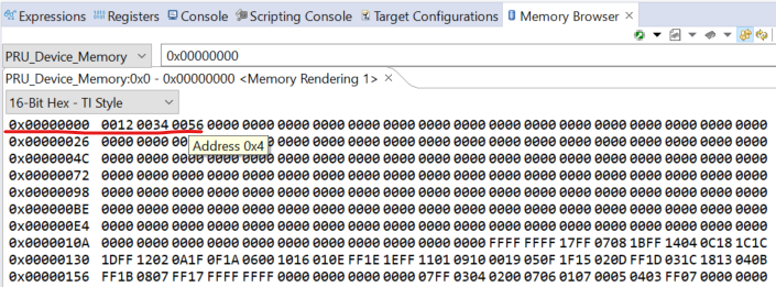
ModeTo verify the accuracy of data transmitting with PRU_GPIO shift mode, 64-bit widths encoded data (0x8000 0012 0034 0056) are sent by the shift-out GPO of the PRU1 core with the first 16-bit 0x8000 (data frame is following the first 1) and received by shift-in GPI of the PRU0 core. The data is then moved from the PRU0 register file to PRU0 RAM from starting address 0x00000000. Both the shift-out and shift-in clock are 125 MHz. Figure 2-8 shows that the PRU1 core received the correct data without errors.
 Figure 2-8 Verification of Data Transmitting
With PRU GPIO Shift Mode