SPRUJ73 December 2023
2.5.1 ADC
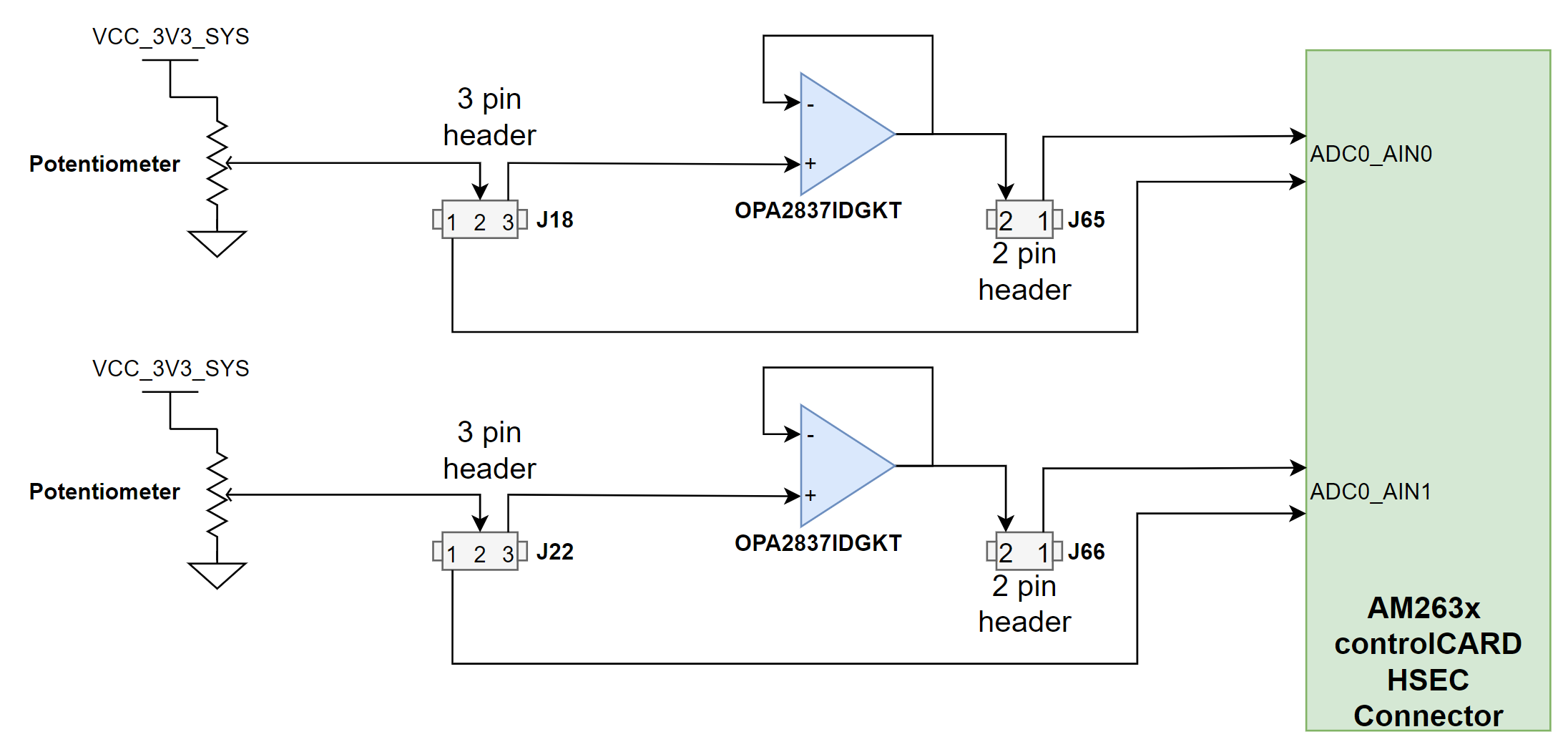
 Figure 2-7 Variable ADC Inputs with Signal Conditioning
The AM263x controlCARD Docking Station is equipped with variable resistors to control the input voltage for ADC channels ADC0_AIN0 and ADC0_AIN1 on the AM263x SoC. Each of these channels is also equipped with an OPA2837IDGKT voltage feedback amplifier for signal conditioning along the ADC input lines. The table below shows the configuration options for these ADC input channels.
| ADC Channel | Header | Jumper Placement | ADC Input Path |
|---|---|---|---|
| ADC0_AIN0 | J18 | No jumper | Potentiometer disconnected from ADC input |
| Pins 2-3 (default) | Potentiometer connected to OPA2837IDGKT | ||
| Pins 1-2 | Potentiometer directly connected to ADC channel input | ||
| J65 | No jumper | Op amp disconnected from ADC input | |
| Pins 1-2 | Op amp connected to ADC channel input | ||
| ADC0_AIN1 | J22 | No jumper | Potentiometer disconnected from ADC input |
| Pins 2-3 (default) | Potentiometer connected to OPA2837IDGKT | ||
| Pins 1-2 | Potentiometer directly connected to ADC channel input | ||
| J66 | No jumper | Op amp disconnected from ADC input | |
| Pins 1-2 | Op amp connected to ADC channel input |
To use the full potentiometer and op-amp signal conditioning path for ADC0_AIN0, a jumper is placed across pins 2 and 3 on J18, and a jumper is placed on pins 1 and 2 on J65. Likewise, for ADC0_AIN1, a jumper is placed across pins 2 and 3 on J22, and a jumper is placed on pins 1 and 2 on J66.
To connect the potentiometer directly to the ADC channel input, a jumper is placed across pins 1 and 2 on J18 and/or J22.