SSZT469A June 2019 – March 2024 TCAN11623-Q1 , TCAN4550-Q1 , TLIN1431-Q1
A system-basis chip (SBC), in its simplest form, is a semiconductor that integrates Controller Area Network (CAN) or Local Interconnect Network (LIN) transceivers with power-management elements. A power-management element could be a low-dropout regulator (LDO), a DC/DC converter, or both.
An SBC can help reduce the elements and transceiver footprint, especially when an application requires additional power or has layout constraints. TI SBCs can also reduce energy consumption in a system, thus extending battery life and reducing power dissipation.
Before diving into SBCs, let’s focus on CAN or LIN transceivers. Both transceivers are bus interfaces that provide communication between various nodes across a cable for their respective technologies. The transceiver takes single-ended information from processor A and converts it to a differential signal that is transmitted across a cable. The receiving transceiver takes the differential signal, converts it back to single ended, and sends it to processor B for further action.
Although there are basic CAN and LIN transceivers on the market, it is possible to enhance them by increasing protection while reducing design complexity, space and cost. These features can often include bus-fault protection, electrostatic discharge protection, and the ability to send and receive data to the processor through a 1.8-V to 3.3-V or 5-V input/output (also known as VIO).
For automotive and industrial designers, the high level of integration and increased reliability of SBCs enable lighter and lower-cost designs for any system that uses CAN or LIN, and a voltage regulator.
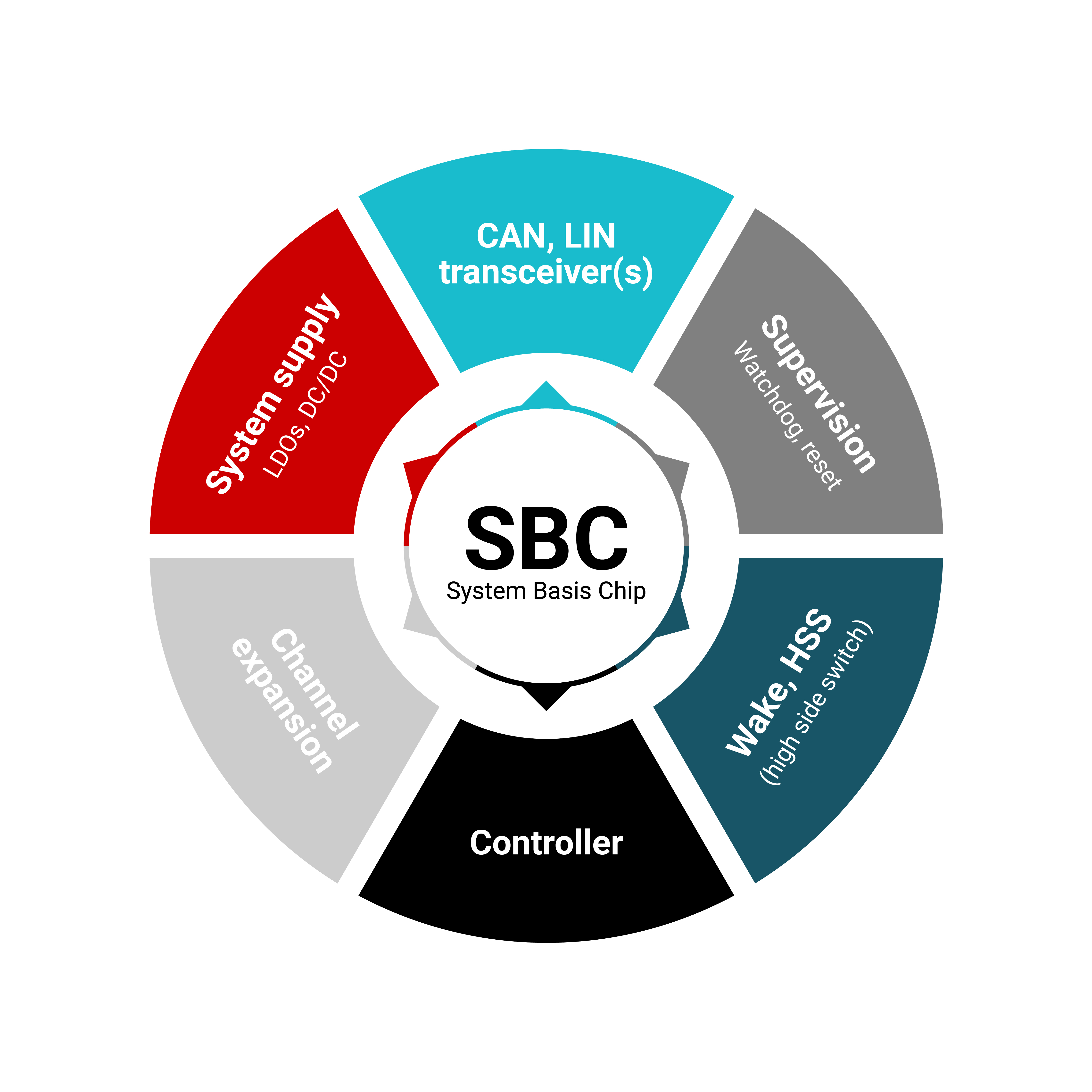
There are three main categories of SBCs, based on the level of integration:
- General-purpose SBCs include a bus interface (CAN, LIN, or both) and an LDO with an output voltage to power other components in the system. This type of SBC could also include a Serial Peripheral Interface (SPI) or pin control for feature configuration from the host, a base watchdog timer, and a wake pin.
- Mid-range SBCs integrate enhanced features that further reduce the board footprint. These features include multiple power elements, high-side switches, multiple wake pins, a limp pin and a configurable watchdog timer. Some will have multiple LIN or CAN transceivers or offer the option to expand the bus interface, with support for channel expansion. The power elements could be DC/DC with >250mA of output current or LDOs that support up to 250mA.
- Advanced SBCs offer special functionalities, which vary based on the overall system’s needs. For example, an integrated CAN controller and transceivers, also known as SPI-to-CAN Flexible Data Rate (FD) controller SBCs, enable easy pairing with hosts that do not have integrated CAN controllers, or hosts that need an additional CAN channel.
 Figure 1 System basis chip
categories
Figure 1 System basis chip
categoriesLet’s review some examples of TI SBCs, their primary features and benefits.
The TCAN11623-Q1general-purpose SBC integrates a CAN FD transceiver; a wake pin; and a 3-V, 70-mA LDO output, while the TCAN11625-Q1 supports a 5-V, 100-mA LDO output. The LDO powers external small loads, while an external component can use the wake pin to wake the node. The TCAN11623-Q1 family of devices has self-supply capability, thus removing the need for an extra voltage rail to power the SBCs.
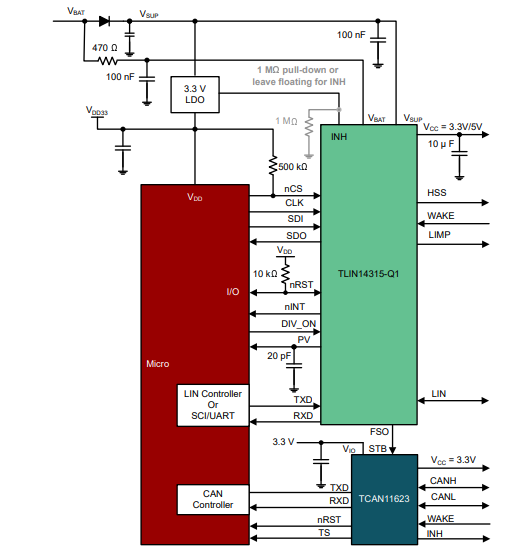
The TLIN1431-Q1 mid-level SBC includes a LIN transceiver, a watchdog timer, a high-side switch, a wake pin and a 125-mA LDO. The TLIN1431-Q1 also supports channel expansion, which gives you the flexibility to expand your system by adding and controlling external LIN or CAN FD transceivers without having to use another general-purpose input/output from the processor. Figure 2 is a basic block diagram of the TLIN1431-Q1 with the TCAN11623-Q1. The channel expansion feature allows the designer to add a CAN channel and another source of power for small loads in the system.
 Figure 2 TLIN1431-Q1 block diagram,
with channel expansion to the TCAN11623-Q1
Figure 2 TLIN1431-Q1 block diagram,
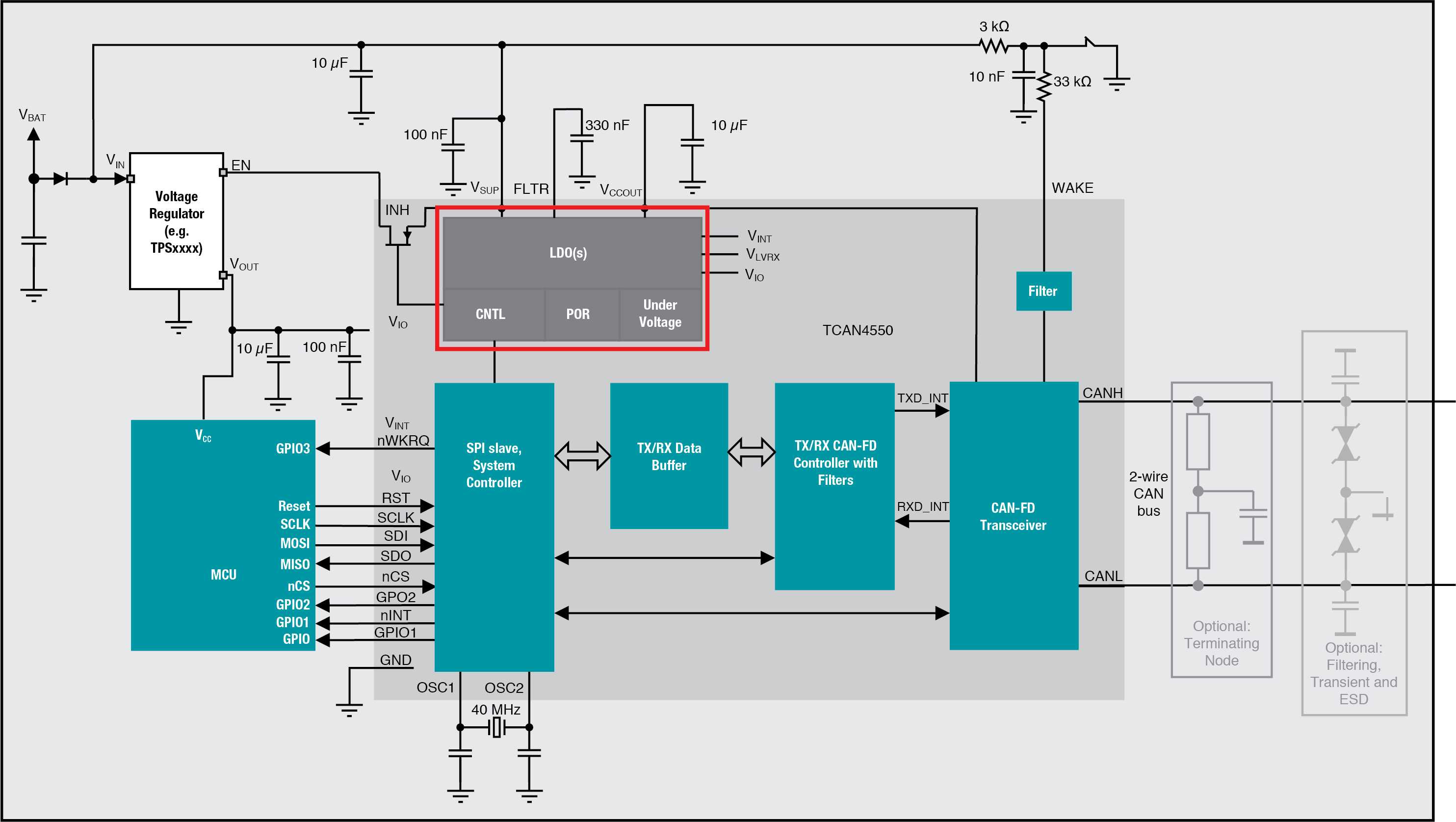
with channel expansion to the TCAN11623-Q1The TCAN4550-Q1 advanced SBC combines both a CAN FD controller and a CAN FD transceiver in a single package. It includes a local wake pin, a watchdog timer and a 70-mA LDO output. The TCAN4550-Q1 adds CAN communication to any host that doesn't have a CAN interface, and allows for an additional CAN channel. It also bridges the gap from classical CAN to CAN FD. Figure 3 shows a basic block diagram of the TCAN4550-Q1 and its connection to a host processor through SPI.
The TCAN4550-Q1 provides additional features, including VIO with 1.8-V, 3.3-V and 5-V support; wake; inhibit; and a timeout watchdog that can enable processor functionality not normally available.
 Figure 3 TCAN4550-Q1 block diagram: processor connections and
integrated LDO
Figure 3 TCAN4550-Q1 block diagram: processor connections and
integrated LDOTI has optimized its CAN and LIN SBCs for board space, system cost and power efficiency. In addition, TI enables designers to meet functional safety compliance through documentation, and to meet automotive original equipment manufacturer emission and manufacturing requirements.
Conclusion
For any system, where you need a bus communication interface, and need to supply power to other components in the system, SBCs are the best solutions. SBCs are available in many options based on transceiver types, output voltages and current sourcing. TI defines the SBC’s architectures to meet a wide range of automotive and industrial application requirements. Designers can configure SBCs, based on their specific system’s needs.
SBCs will evolve based on market needs, powered by CAN and LIN standards to meet the needs of an ever-changing market environment.
Additional Resources
- For information about the integrated LDO in the TCAN4550-Q1, see the application report, “Understanding LDO Performance in the TCAN4550-Q1.".
- Read the technical article, "Discrete SBCs: Versatile and Scalable Solutions for Any Application".
- Read the technical article, "Explore the non-speed-related benefits of CAN FD."